Polishing device

a technology of polishing device and polishing rate, which is applied in the direction of grinding drive, manufacturing tools, lapping machines, etc., can solve the problems of reducing the product yield of the resultant semiconductor device, degrading the polishing rate, etc., to prevent the occurrence of insufficient downward pressure, improve the uniformity of the polishing device, and prevent the effect of reducing the polishing ra

Active Publication Date: 2007-11-22
MICRON TECH INC
View PDF9 Cites 7 Cited by
  • Summary
  • Abstract
  • Description
  • Claims
  • Application Information

AI Technical Summary

Benefits of technology

[0011]In view of the above, it is an object of the present invention to provide a polishing device capable of preventing the reduction of the polishing rate to improve the within-wafer uniformity of the polishing device by preventing occurrence of an insufficient downward pressure in the vicinity of the periphery of the wafer.

Problems solved by technology

The insufficient downward pressure in the peripheral area leads to lowering of the polishing rate and causing an insufficient within-wafer uniformity in the wafer 12 after the polishing process, thereby degrading the product yield of the resultant semiconductor devices.

Method used


Image

  • Polishing device
  • Polishing device
  • Polishing device

Examples


Embodiment Construction

[0023]Now, an exemplary embodiment of the resent invention will be described with reference to accompanying drawings, wherein similar constituent elements are designated by similar reference numerals throughout the drawings.

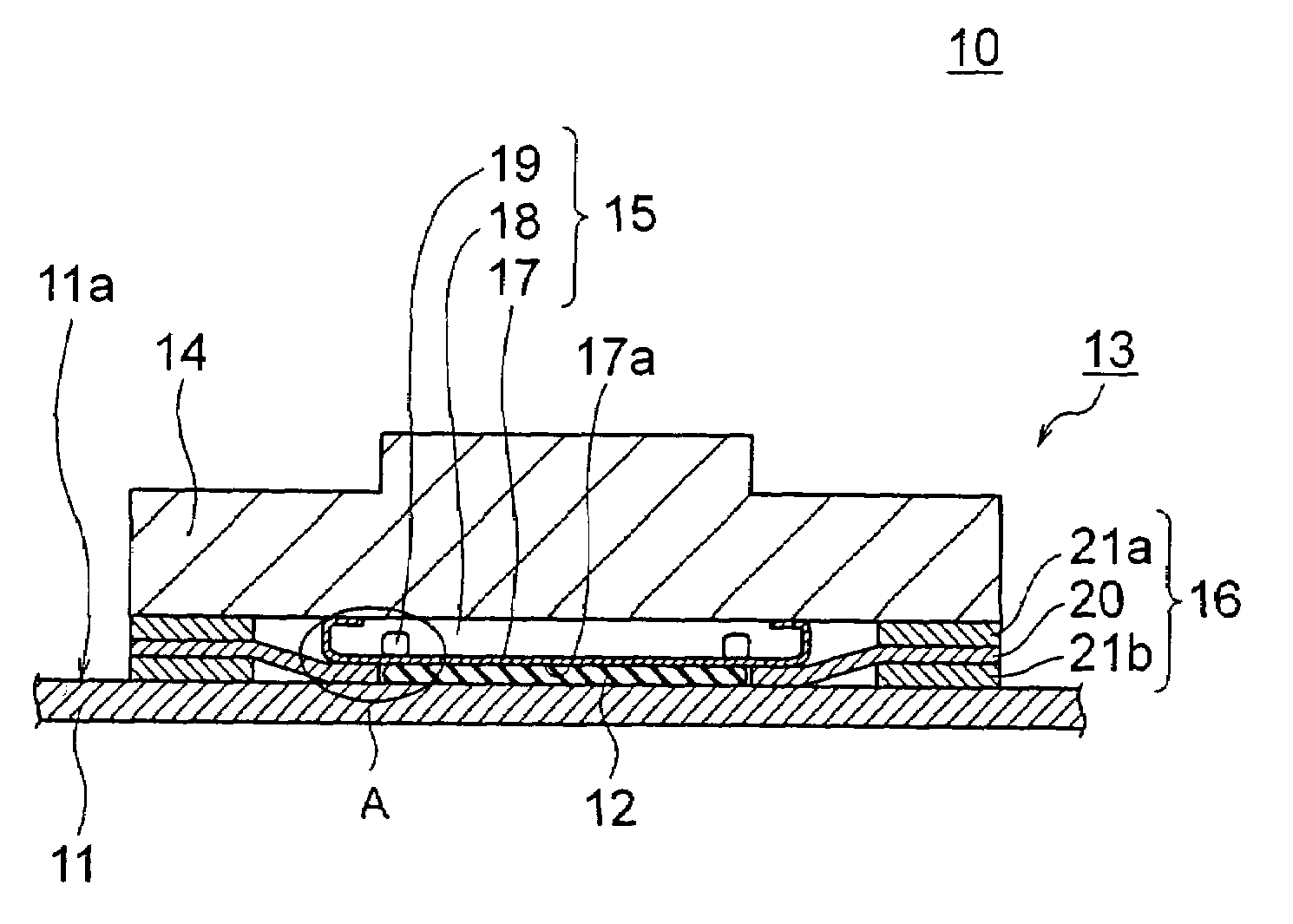
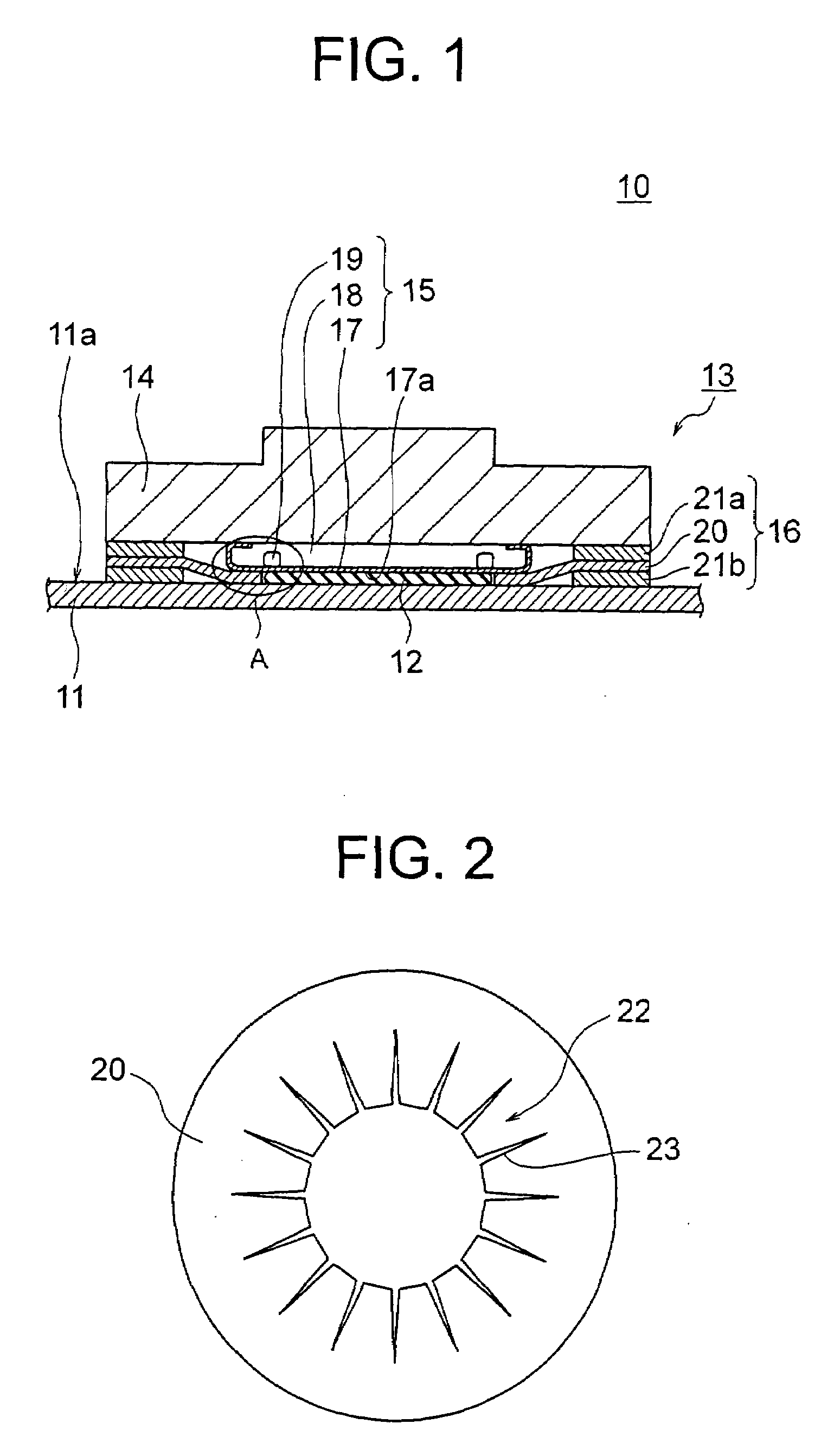
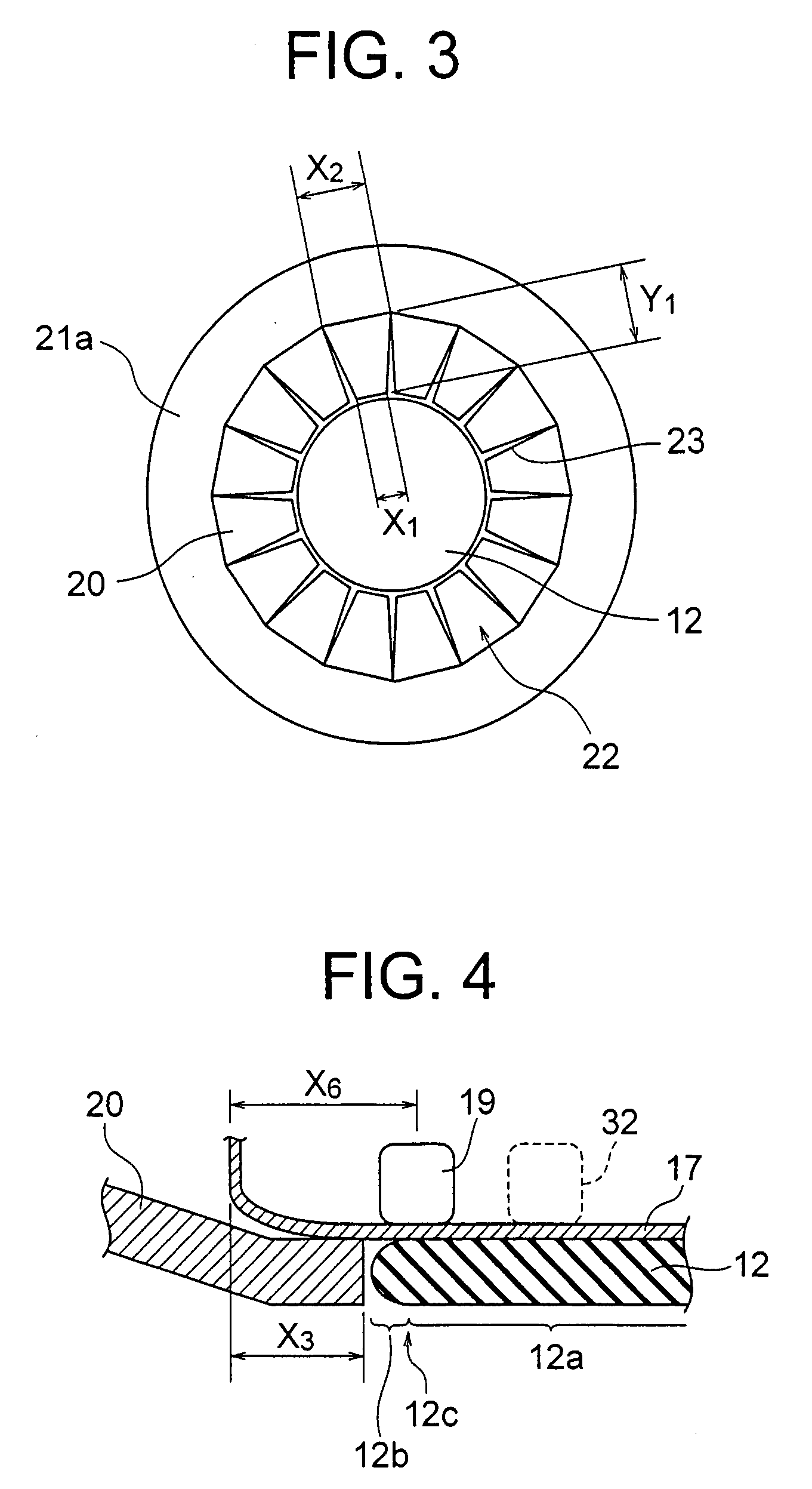
[0024]FIG. 1 shows the polishing device of the exemplary embodiment, generally designated at numeral 10, for use in a CMP process in a semiconductor device manufacturing process. The polishing device 10 includes a polishing pad 11, which includes a circular polishing surface 11a and is rotated about the center thereof. The polishing pad 11 is made of polyurethane, and has thereon a plurality of grooves (not shown) used for polishing the wafer 12.

[0025]The tip portion of a tube (not shown) for supplying therethrough slurry is supported on the polishing pad 11 such that the slurry is supplied onto the center of the polishing surface 11a. The polishing device 100 includes a polishing head 13 opposing the polishing surface 11a with the wafer 12 being sandwiched there...


PUM


Abstract

A polishing device includes a polishing pad for polishing a wafer and a polishing head for holding the wafer. The polishing head has a retainer ring for retaining the wafer in the in-plane direction of the wafer, a membrane sheet for pressing the wafer against the polishing pad, and a head body for supporting the retainer ring and the membrane sheet. The retainer ring has a subordinate retainer member having a ring portion and a plurality of fins extending from the ring portion to retain the peripheral surface of the wafer. The subordinate retainer member has a thickness equal to the thickness of the wafer. The membrane sheet has a diameter larger than the wafer, and presses the wafer and the vicinity of the inner edge of the subordinate retainer member.

Description

[0001]This application is based upon and claims the benefit of priority from Japanese patent application No. 2006-136024 filed on May 16, 2006, the disclosure of which is incorporated herein in its entirety by reference.BACKGROUND OF THE INVENTION[0002]1. Field of the Invention[0003]The present invention relates to a polishing device. In particular, the present invention relates to a polishing device for use in a chemical-mechanical-polishing (CMP) process in manufacturing a semiconductor device.[0004]2. Description of the Related Art[0005]In recent years, since the density for integration of a semiconductor device has been increased, the number of interconnection layers in a multilayer interconnection structure is increased in the semiconductor device. In a photolithographic process for the semiconductor device having the multilayer interconnection structure, the uniformity of the film surface exposed by an exposure system should correspond to the range of focal depth of the light ...

Claims


Application Information

Patent Timeline
Patent Type & Authority Applications(United States)
IPC IPC(8): B24B29/00B24B37/005B24B37/04B24B37/30H01L21/304
CPCB24B37/30
Inventor SAITO, TOSHIYA
Owner MICRON TECH INC
Why Eureka
Try Eureka