Solid-state image sensing device and manufacturing method thereof

Inactive Publication Date: 2007-11-29
COLLABO INNOVATIONS INC
View PDF3 Cites 21 Cited by
  • Summary
  • Abstract
  • Description
  • Claims
  • Application Information

AI Technical Summary

Benefits of technology

[0013]It can be seen from FIG. 1B that a slightly declined part appears in the profile of the potential distribution for the implantation energy of 400 KeV, and a greatly declined part appears in the profile of the potential distribution for the implantation energy of 600 KeV. Therefore, it can be understood that as the implantation energy increases, in other words, the charge storage portion 14 deepens, a declined part in the profile of the potential distribution becomes more apparent and deeper.
[0035]Moreover, according to the solid-state image sensing device of the present invention, the buried gate surrounds the entire charge storage portion, so that a higher effectiveness in suppressing residual image can be obtained. This allows a deep charge storage portion with an increased density. As a result, it is possible to miniaturize the solid-state image sensing device.

Problems solved by technology

The deep charge storage portion may cause a problem, that is, cross talk.
However, inventers of the present invention found that forming a deep photodiode might cause a novel problem besides the cross talk.
The novel problem found by the inventors is that in a deep photodiode, a voltage applied to a transfer gate can not completely transfer a voltage stored in the photodiode to a floating diffusion portion, which causes a residual image.

Method used


Image

  • Solid-state image sensing device and manufacturing method thereof
  • Solid-state image sensing device and manufacturing method thereof
  • Solid-state image sensing device and manufacturing method thereof

Examples


embodiment 1

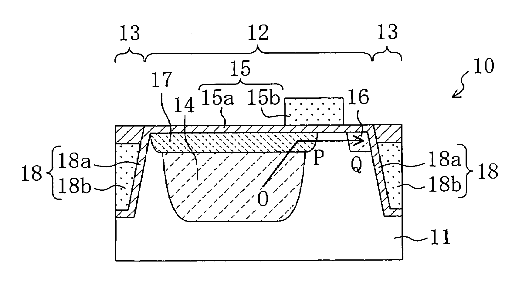
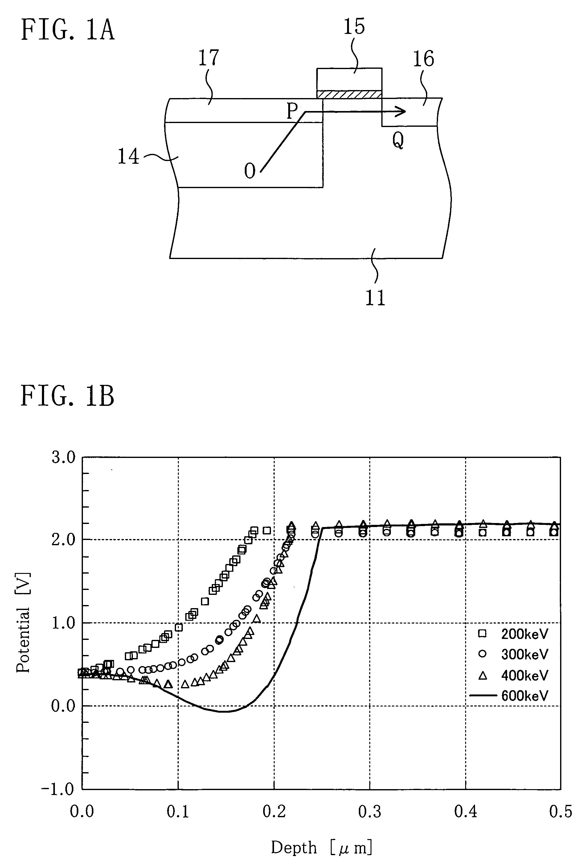
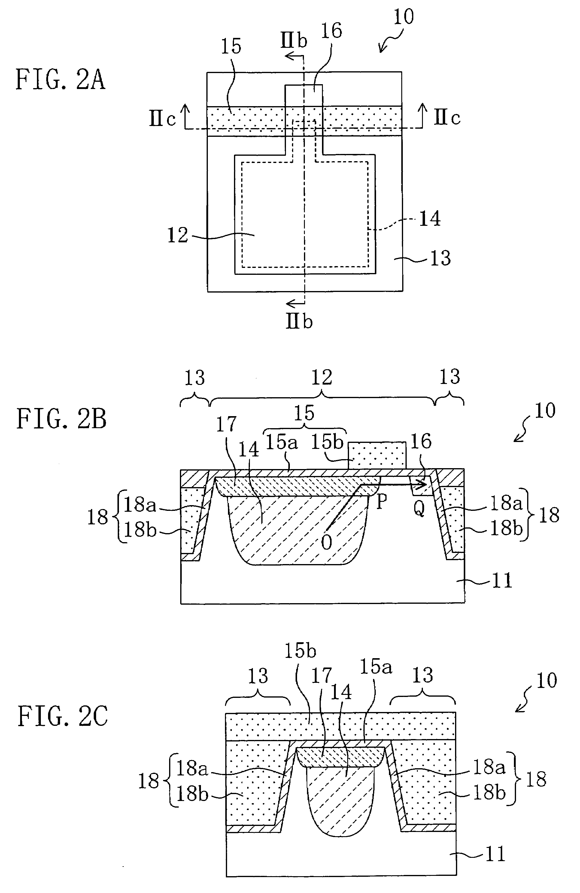
[0053]In FIGS. 2A through 2C, a structure of a solid-state image sensing device 10 according to Embodiment 1 of the present invention is schematically shown, where FIG. 2A is a plan view of the solid-state image sensing device 10, FIG. 2B is a cross section along the line IIb-IIb in FIG. 2A, and FIG. 2C is a cross section along the line IIc-IIc in FIG. 2A.

[0054]As shown in FIGS. 2A through 2C, in the solid-state image sensing device 10 according to Embodiment 1, pixel portions 12 each of which has a charge storage portion 14 in a semiconductor substrate 11 and a transfer gate 15 for transferring charges stored in the charge storage portion 14 are isolated from each other by a device isolation region 13 in the semiconductor substrate 11, and a buried gate 18 which is electrically connected to the transfer gate 15 is provided in the device isolation region 13.

[0055]As shown in FIG. 2B, the transfer gate 15 includes a gate dielectric film (second gate dielectric film) 15a and a gate el...

embodiment 2

[0083]FIGS. 10A through 10C schematically illustrate a structure of a solid-state image sensing device 20 according to Embodiment 2 of the present invention, where FIG. 10A is a plan view of the solid-state image sensing device 20, FIG. 10B is a cross section along the line Xb-Xb in FIG. 10A, and FIG. 10C is a cross section along the line Xc-Xc in FIG. 10A.

[0084]In Embodiment 1, the buried gate 18 embedded in the device isolation region 13 surrounds the charge storage portion 14. Compared to this, in a structure in Embodiment 2, a buried gate 18 is formed in a part of a device isolation region 13. This structure is especially effective, for example, in a case shown in FIG. 10A where it is difficult to provide a gate electrode 18b of the buried gate 18 in a region having a narrow width (a region where a transfer gate is not formed) in the device isolation region 13.

[0085]As shown in FIG. 10B, a transfer gate 15 includes a gate dielectric film (second gate dielectric film) 15a and a g...


PUM


Abstract

Pixel portions each of which has a charge storage portion formed in a semiconductor substrate 11 and a transfer gate for transferring charges stored in the charge storage portion are isolated from each other by a device isolation region in the semiconductor substrate. A buried gate electrically connected to the transfer gate is embedded in the device isolation region. The buried gate includes a gate dielectric film and gate electrode formed in a trench of the semiconductor substrate.

Description

CROSS-REFERENCE TO RELATED APPLICATION(S)[0001]This application claims priority under 35 U. S. C. §119(a) on Japanese Patent Application No. 2006-146879 filed on May 26, 2006, the entire contents disclosed in claims, specification, and drawings of which are hereby incorporated by reference.BACKGROUND OF THE INVENTION[0002]1. Field of the Invention[0003]The present invention relates to a solid-state image sensing device and a manufacturing method thereof. Specifically, the present invention relates to a solid-state image sensing device and a manufacturing method thereof in which miniaturization of device does not deteriorate image properties.[0004]2. Description of the Prior Art[0005]In recent years, among solid-state image sensing devices, a solid-state image sensing device using an amplification-type MOS sensor has been a subject of interest. In this solid-state image sensing device, a signal detected by a photodiode is amplified by a transistor on a pixel to pixel basis. Such soli...

Claims


Application Information

Patent Timeline
IPC IPC(8): H01L31/113H01L27/146H04N5/335H04N5/341H04N5/357H04N5/369H04N5/372H04N5/374
CPCH01L27/14603H01L27/14689H01L27/1463
Inventor MISAKI, MAKOTOTSUTSUI, MASAFUMI
Owner COLLABO INNOVATIONS INC
Why Eureka
Try Eureka