
Piezoelectric device

a piezoelectric device and piezoelectric technology, applied in piezoelectric/electrostrictive/magnetostrictive devices, piezoelectric/electrostriction/magnetostriction machines, electrical apparatus, etc., can solve the problem of thin devices, breakage of ic chips or packages, and difficulty in realizing thin piezoelectric devices in the related art structure, etc. problem, to achieve the effect of reducing thickness

Inactive Publication Date: 2007-11-29
SEIKO EPSON CORP
View PDF8 Cites 25 Cited by
  • Summary
  • Abstract
  • Description
  • Claims
  • Application Information

AI Technical Summary

Benefits of technology

[0007]An advantage of the present invention is to provide a piezoelectric device realizing thickness reduction thereof without undergoing warpage and breakage of an IC chip or a package thereof.
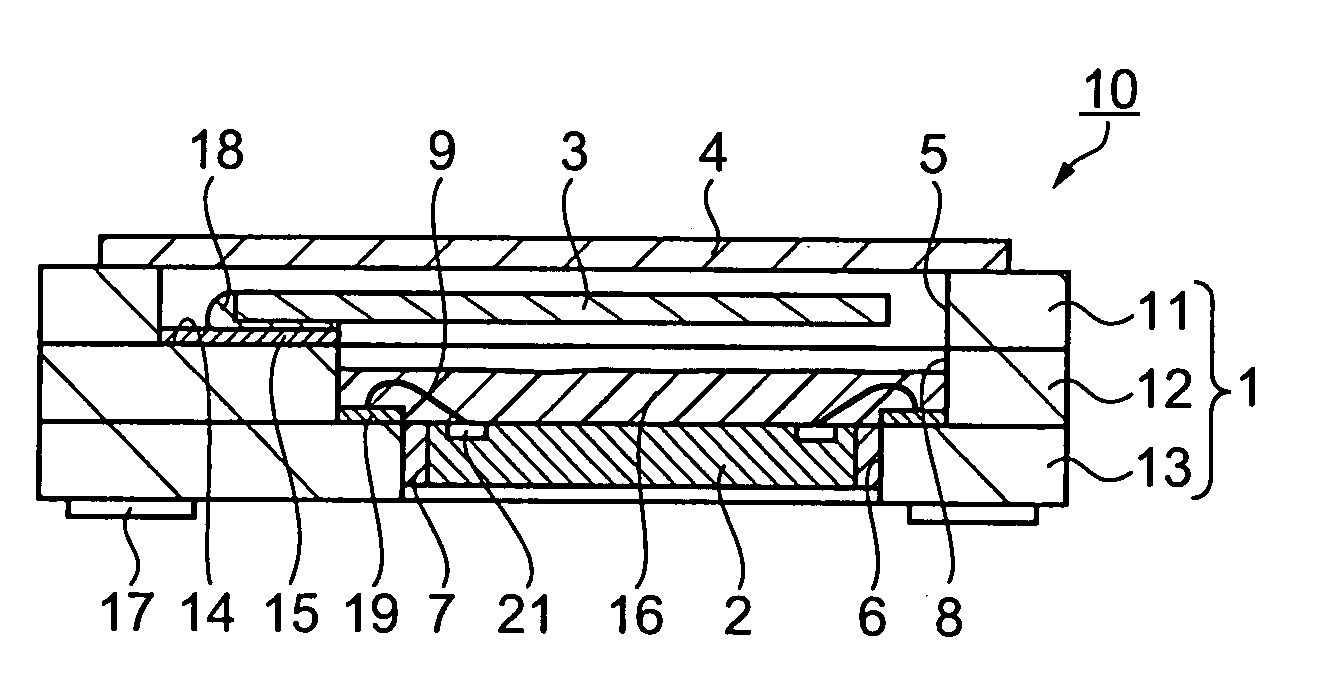
[0008]A piezoelectric device according to an aspect of the invention includes: a package having a first recessed part provided on a first surface, a second recessed part provided on a second surface, and a penetrating part passing partially from the first recessed part through the second recessed part; a piezoelectric element housed in the first recessed part; a lid disposed on the upper side of the first recessed part; an IC chip disposed and fixed in the second recessed part of the package so as to block a part of the penetrating part; and a sealing part provided to the second recessed part. The IC chip and the sealing part close up the penetrating part, and the lid seals the first recessed part air-tightly.
[0009]In this structure, the IC chip is disposed and fixed in the second recessed part by an adhesive made of resin having bonding power, such as epoxy resin so as to block at least a part of the penetrating part formed in the package. Then the sealing part made of resin having bonding power such as epoxy resin, is provided to a space surrounding the lateral faces of the IC chip in the second recessed part. Thus, the penetrating part is closed up by the IC chip and the sealing part. The IC chip is disposed in the second recessed part. Therefore, compared to the related art structure in which the IC chip is disposed on the bottom surface of the package recessed part forming the housing recessed part, the quartz crystal oscillator realizes the thickness reduction thereof by the thickness of the bottom of the housing recessed part without undergoing warpage and breakage of the IC chip or the package.
[0010]In the piezoelectric device of the aspect, at least one lateral face of the second recessed part may be opened.
[0011]In this structure, the second recessed part can house a larger IC chip than the IC chip housed in the related art housing recessed part.

Problems solved by technology

However, making the devices thinner causes warpage and breakage of the IC chip or the package.
Thus, it is difficult to realize thinner piezoelectric devices in the related art structure.

Method used


Image

  • Piezoelectric device
  • Piezoelectric device
  • Piezoelectric device

Examples


first embodiment

[0018]A first embodiment illustrates a quartz crystal oscillator as a piezoelectric device.

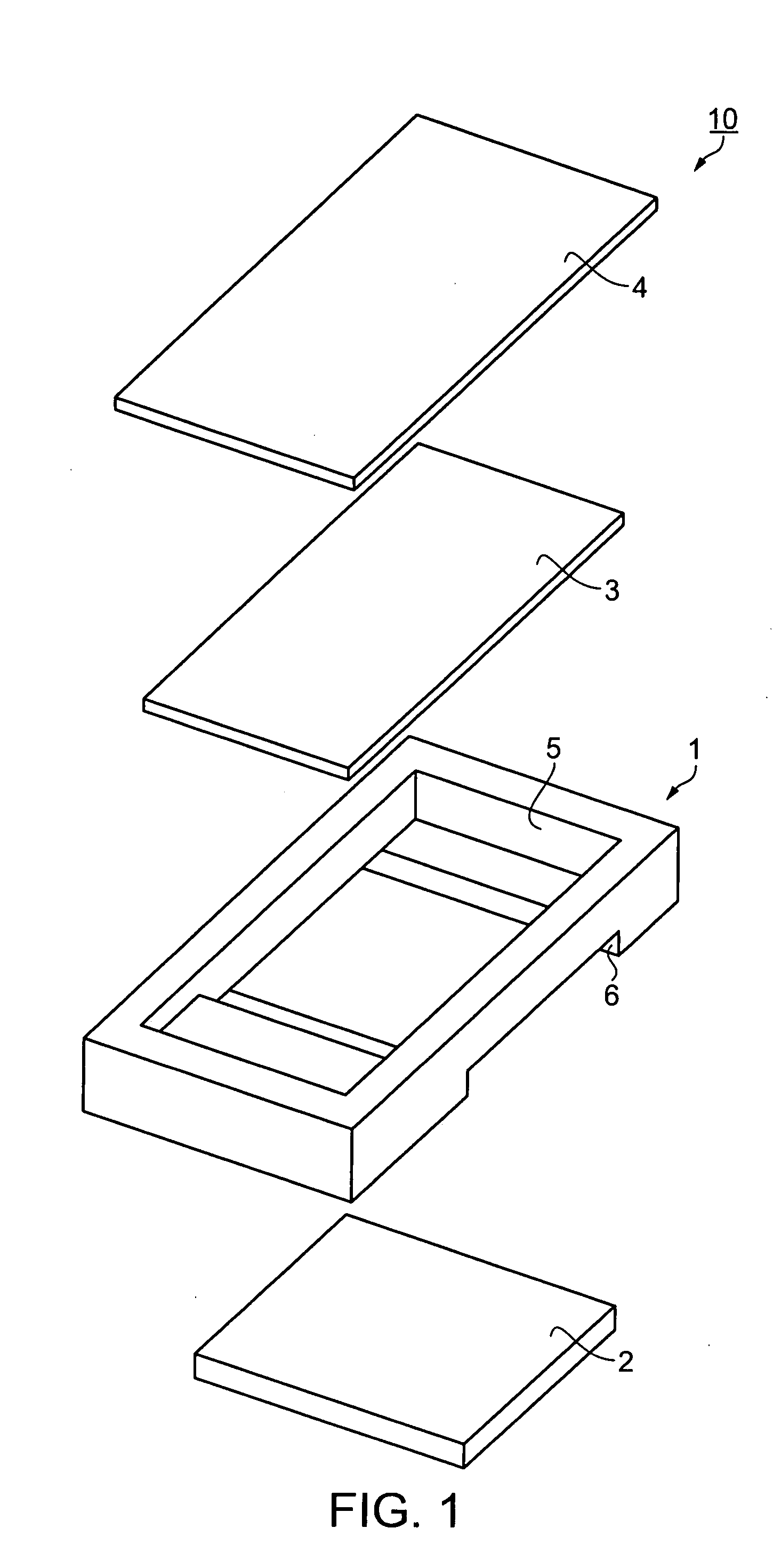
[0019]FIG. 1 is an exploded perspective view showing components of this quartz crystal oscillator of the first embodiment.

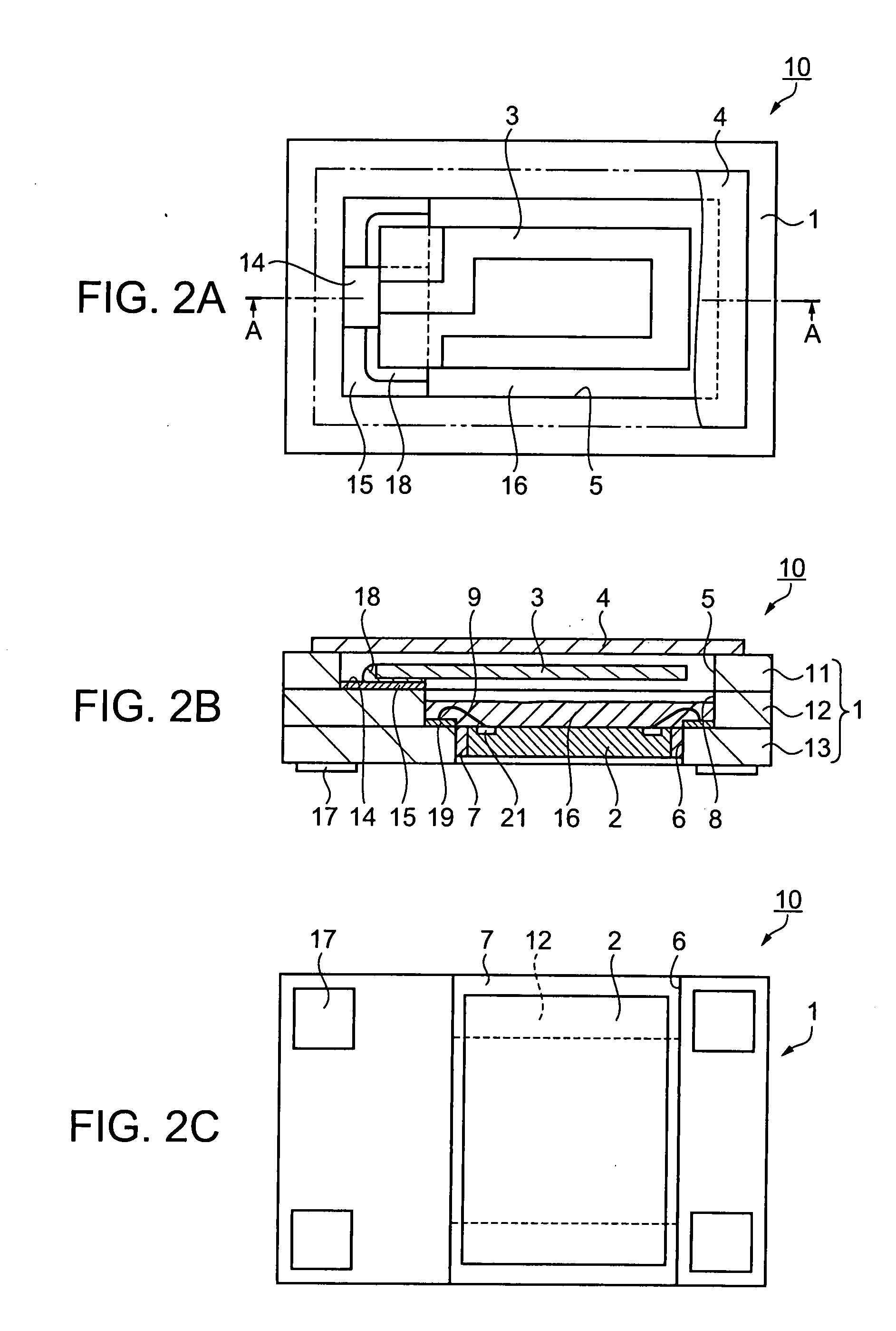
[0020]FIGS. 2A to 2C show a structure of the quartz crystal oscillator of the first embodiment. FIG. 2A is a schematic plan view, FIG. 2B is a schematic sectional view taken along the line A-A of FIG. 2A, and FIG. 2C is a schematic bottom plan view of FIG. 2A.

[0021]As shown in FIG. 1, this quartz crystal oscillator 10 is provided with a package 1 made of ceramic and the like, a quartz crystal resonator 3 as a piezoelectric element, an IC chip 2 having a function, for example, to oscillate the quartz crystal resonator 3, and a lid 4 made of metal and the like. Further, the package 1 is provided with a first recessed part 5 on a first surface, and a second recessed part 6 on a second surface making up the front and rear sides of the package 1 along with the first surface.

[002...

second embodiment

[0039]FIGS. 4A to 4C show a structure of a surface acoustic wave (SAW) oscillator of a second embodiment. FIG. 4A is a schematic plan view, FIG. 4B is a schematic sectional view taken along the line C-C of FIG. 4A, and FIG. 4C is a schematic bottom plan view of the FIG. 4A.

[0040]In this SAW oscillator 30, an SAW resonator 33 as a piezoelectric element is fixed by an adhesive and coupled by a metal wire, while the quartz crystal resonator as a piezoelectric element is fixed and coupled by the conductive adhesive in the first embodiment. Other elements have the same structure as the ones of FIGS. 2A to 2C in the first embodiment to be given the same reference numbers, and the description thereof is omitted.

[0041]The SAW oscillator 30 is provided with a package 31 made of ceramic and the like, the SAW resonator 33 as a piezoelectric element, an IC chip 2 having a function, for example, to oscillate the SAW resonator 33, and a lid 4 made of metal and the like. Further, the package 31 is...


PUM


Abstract

A piezoelectric device includes: a package including a first recessed part provided on a first surface of the package, a second recessed part provided on a second surface of the package, and a penetrating part passing partially from the first recessed part through the second recessed part; a piezoelectric element housed in the first recessed part; a lid disposed on the upper side of the first recessed part; an IC chip disposed and fixed in the second recessed part of the package so as to block a part of the penetrating part; and a sealing part provided to the second recessed part. The IC chip and the sealing part close up the penetrating part and the lid seals the first recessed part air-tightly. A piezoelectric device is provided. The piezoelectric device realizes thickness reduction thereof without undergoing warpage and breakage of an IC chip or a package thereof.

Description

BACKGROUND[0001]1. Technical Field[0002]The present invention relates to a piezoelectric device.[0003]2. Related Art[0004]Piezoelectric devices are provided with a piezoelectric resonator typified by a quartz crystal resonator, and an oscillation circuit. The piezoelectric devices have conventionally been used as clock frequency sources of various electronic apparatuses such as a personal computer or a mobile communication device.[0005]As electronic apparatuses mounting piezoelectric devices are miniaturized and thinned, the piezoelectric devices are also required to be further miniaturized and thinned. For example, JP-A-3-272207, FIG. 1, pp. 4-6 discloses a piezoelectric device. The piezoelectric device has such structure that an IC chip is disposed in a housing recessed part formed in a package made of ceramic, a piezoelectric element is disposed above the IC chip, and the housing recessed part is sealed air-tightly by a lid.[0006]In the structure of the related art piezoelectric ...

Claims


Application Information

Patent Timeline
IPC IPC(8): H03H9/10
CPCH03H9/1021H03H9/0547
Inventor NARUSE, HIDETO
Owner SEIKO EPSON CORP
Learn More