Organic el light-emitting device and electronic apparatus

a light-emitting device and light-emitting device technology, applied in the direction of organic semiconductor devices, discharge tubes/lamp details, discharge tubes luminescent screens, etc., can solve the problems of difficult to provide a dielectric mirror over the luminescent layer, difficult to provide a dielectric mirror in the top emission type, damage to the underlying layer, etc., to achieve a wide color specification range and enhance monochromaticity

Active Publication Date: 2007-11-29
SEIKO EPSON CORP
View PDF11 Cites 29 Cited by
  • Summary
  • Abstract
  • Description
  • Claims
  • Application Information

AI Technical Summary

Benefits of technology

[0009]In this structure, light having a specific wavelength of the light reflected from the semi-transparent semi-reflective layer is strengthened in the dielectric mirror formed under the function layer and is then emitted to the outside. This structure allows the dielectric mirror to be provided in a top emission EL device. Consequently, the organic EL light-emitting device has long lifetime or low power consumption, and besides exhibits high monochromaticity.
[0027]Since the organic EL light-emitting devices for three primary color lights each emit light with enhanced monochromaticity, a display device displaying high-quality mages in a wider color specification range can be achieved.

Problems solved by technology

However, the dielectric mirror is formed by repeating the deposition of thin layers, so that the underlying layer is damaged by, for example, heating.
It is therefore difficult to provide a dielectric mirror over the luminescent layer, which is made of an organic material.
Thus it is difficult to provide a dielectric mirror in a top emission type, which emits light from the upper side of the luminescent layer.
Such a dielectric mirror prevents reduction in reliability and increase in manufacturing cost, and increases the intensity of light having a specific wavelength.

Method used


Image

  • Organic el light-emitting device and electronic apparatus
  • Organic el light-emitting device and electronic apparatus
  • Organic el light-emitting device and electronic apparatus

Examples


first embodiment

[0062]FIGS. 3A to 6 show a light-emitting device according to a first embodiment of the invention line head including the light-emitting devices, and an image-forming apparatus (printer) being an electronic apparatus including the line heads.

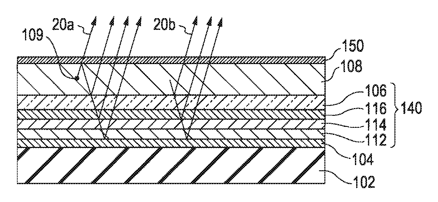
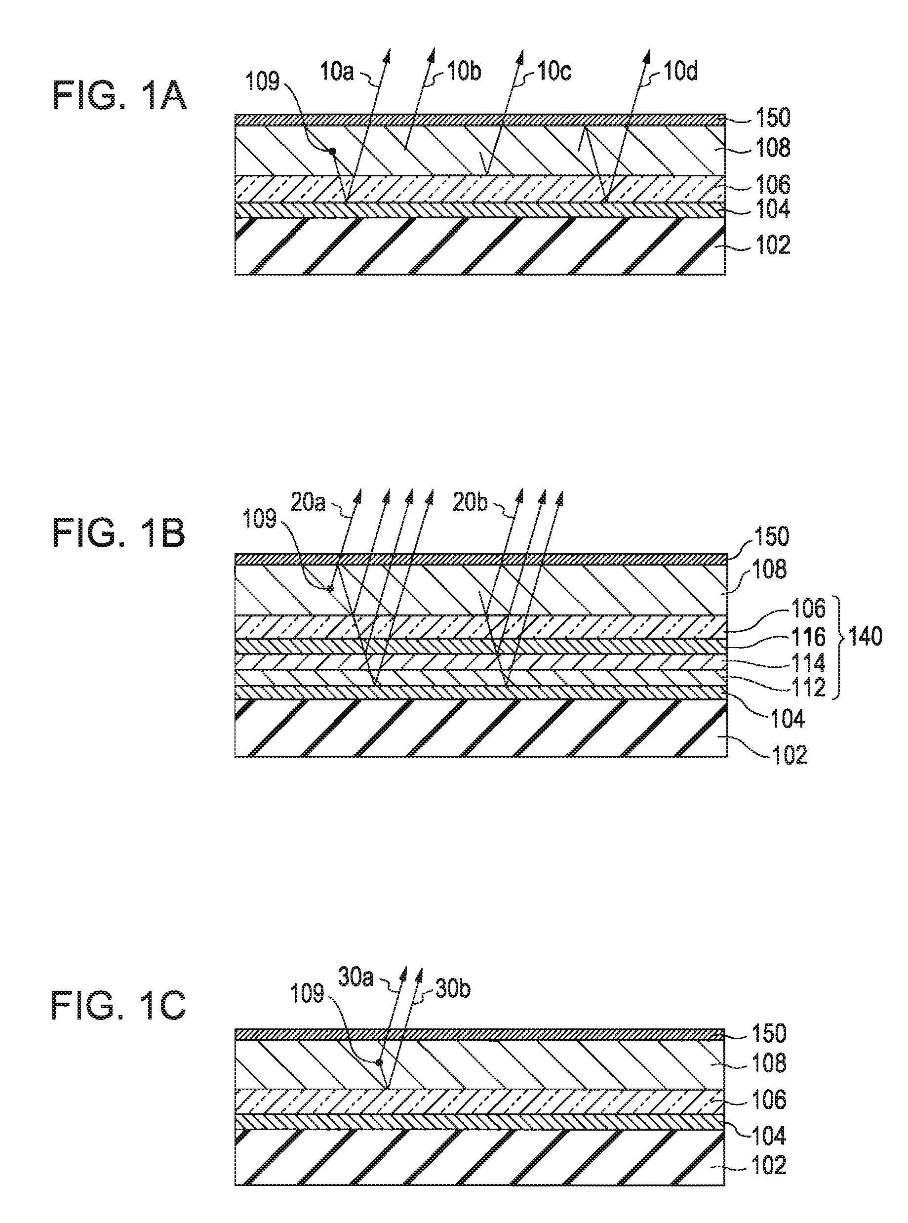
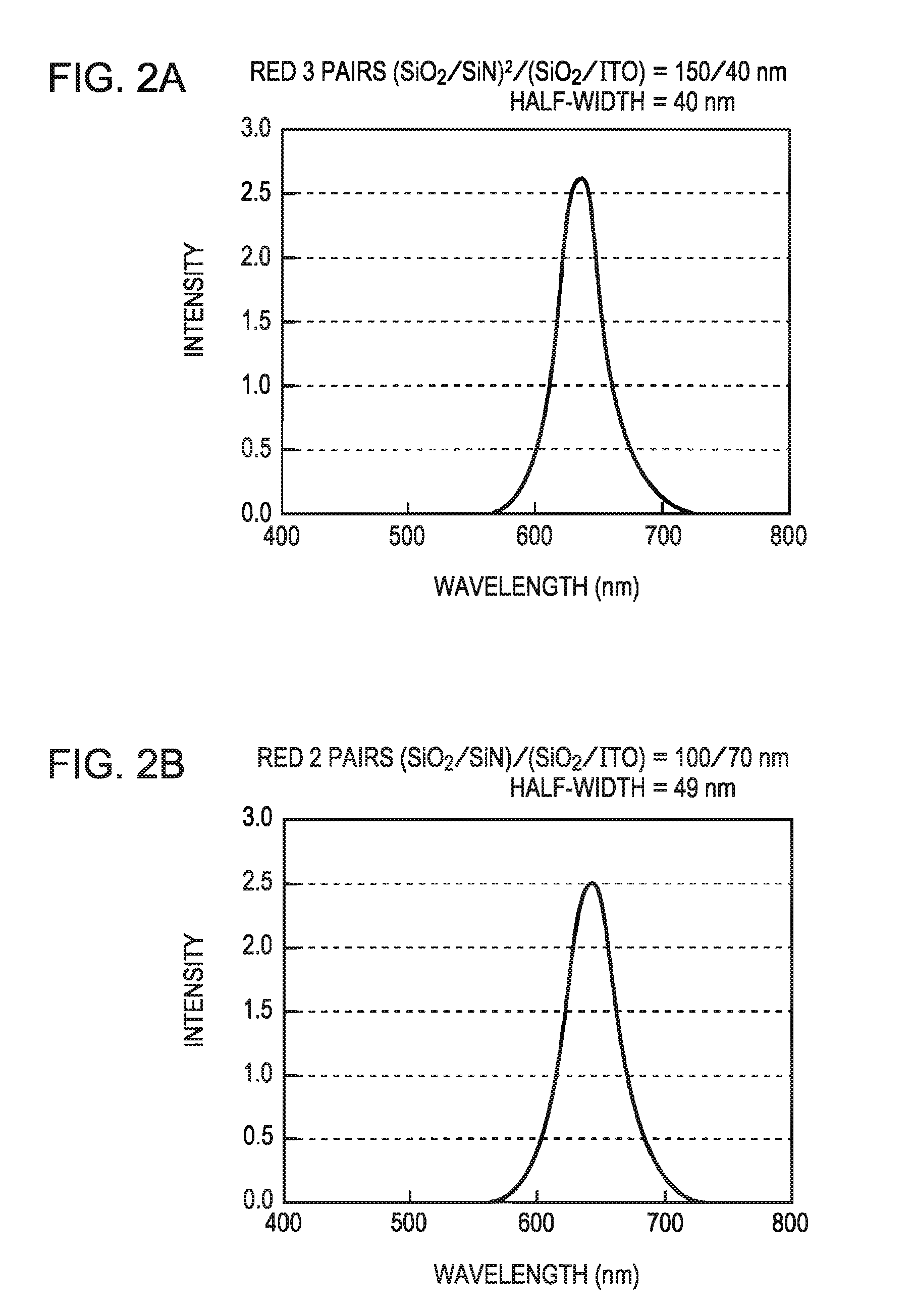
[0063]FIG. 3A is a sectional view of the light-emitting device 72 according to the present embodiment with a driving thin film transistor (hereinafter referred to as TFT) 412. FIG. 3B is an enlarged view of portion A shown in FIG. 3A. The light-emitting device 72 is of too emission type. The substrate 101 is therefore not necessarily optically transparent, and can be made of glass, ceramic, a metal, or any other material. The light-emitting device 72 is formed on an insulating layer 102 that is formed on the substrate 101 with a plurality of layers in between. The insulating layer 102 is intended to separate the TFT 412 from the light reflection layer and the pixel electrode, and is formed by CVD of silicon oxide. The TFT 412 is prepared by a kn...

second embodiment

[0081]FIGS. 7 to 12 show a light-emitting device according to a second embodiment of the invention, an organic LE display device (hereinafter referred to as the display device) being an electronic apparatus including the light-emitting device, and a mobile personal computer including the display device.

[0082]FIG. 7 is an entire circuit diagram of a display device according to the present embodiment. The display device is of active matrix type that includes three types of light-emitting devices arranged in a matrix manner, each independently controlled to emit red, green, or blue light. The display device is broadly divided into an image display region and a peripheral region. The image display region 70 has a plurality of scanning lines 702, a plurality of signal lines 704 orthogonal to the scanning lines 702, and a plurality of power supply lines 706 extending parallel to the signal lines 704. Scanning line driving circuits 720 and a signal line driving circuit 730 are disposed aro...


PUM


Abstract

A top emission organic EL light-emitting device on a substrate is provided which emits light from the side opposite the substrate. The organic EL light-emitting device includes a light reflection layer, a first electrode made of a transparent conductive material, a function layer including an organic EL luminescent layer that emits light, and a second electrode disposed in that order on the substrate. The second electrode includes a semi-transparent semi-reflective layer that transmits part of the light emitted from the organic EL luminescent layer and reflects the rest of the light. The organic EL light-emitting device also includes a dielectric mirror disposed between the function layer and the light reflection layer. The dielectric mirror acts as an optical resonator that strengthens light having a specific wavelength.

Description

BACKGROUND[0001]1. Technical Field[0002]The present invention relates to an organic EL light-emitting device and an electronic apparatus including the light-emitting device.[0003]2. Related Art[0004]EL (electroluminescence) light-emitting devices, particularly organic EL light-emitting devices, feature the ease of reducing the weight and thickness, and are increasingly being used as image forming elements of a display or as light-emitting pixels of an image-forming apparatus that transfers an image formed with a line head module to a medium with a photosensitive drum.[0005]It is desired that monochromaticity is increased in order to increase the color specification range in the field of displays, and in order to prevent the degradation (blur) of formed images resulting from wavelength dispersion of the SELFOC® lens array used in imaging optical systems in the field of image-forming apparatuses. For example, Japanese Unexamined Patent Application Publication No. 06-275381 has disclos...

Claims


Application Information

Patent Timeline
Patent Type & Authority Applications(United States)
IPC IPC(8): H01J1/62
CPCH01L2251/5315H01L51/5265H10K50/852H10K2102/3026H05B33/22
Inventor KOBAYASHI, HIDEKAZU
Owner SEIKO EPSON CORP
Why Eureka
Try Eureka