Organic light emitting device

a light-emitting device and organic technology, applied in the direction of discharge tube luminescnet screens, electric discharge lamps, electrical equipment, etc., can solve the problems of fracture sensitivity of oleds, thereby exacerbated difficulty, and the subject of intensive development work of oleds, and achieve small structural height and sufficient stability.

Inactive Publication Date: 2007-11-29
SCHOTT AG
View PDF10 Cites 18 Cited by
  • Summary
  • Abstract
  • Description
  • Claims
  • Application Information

AI Technical Summary

Benefits of technology

[0020] A further object of the invention is to provide an OLED having a patterned luminous area that is cost-effective and s simple to produce.
[0048] It is furthermore advantageous for one or more end sides of the layers of the organic light emitting device to be beveled in order to obtain, toward the front, an edge coupling-out of light and thus a luminous border.

Problems solved by technology

OLEDs are therefore the subject of intensive development work.
However, this advantage of the small thickness is accompanied by a difficulty, namely the fracture sensitivity of an OLED.
This difficulty is thereby also considerably exacerbated insofar as glass substrates are used.
Particularly in areas in which an OLED is to be handled by a user, e.g. in the case of mechanically stressed display applications that come into contact with the body, this gives rise to a potential risk of injury.
Said current leads to high emission of electromagnetic fields at the large-area electrodes.
Furthermore, relatively high voltages are used.
This once again results in multiple potential endangering of the user.
However, these technologies have in common the serious disadvantage that the patterning requires special and complicated manufacturing technologies and the patterning usually even has to be carried out under clean room conditions.
Furthermore, the known technologies are extremely inflexible since even in the production of the OLED layer arrangement it is necessary to perform the patterning within the OLED.
To summarize, the technologies are suitable only to a limited extent for a series of mass applications involving specific safety requirements, on the one hand, and a considerable cost pressure, on the other hand.

Method used


Image

  • Organic light emitting device
  • Organic light emitting device
  • Organic light emitting device

Examples


Embodiment Construction

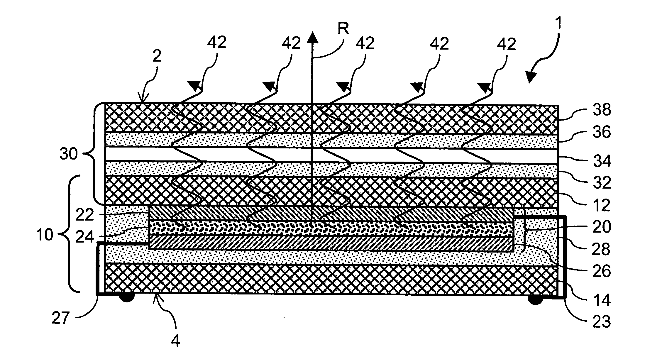
[0057]FIG. 1 shows an unpatterned organic light emitting device 1. The device 1 comprises a light emitting composite element 10 with a transparent base substrate 12 made of glass, onto which an organic light emitting layer arrangement 20 is applied or deposited, and with a covering substrate 14. The light emitting layer arrangement 20 in turn comprises a light emitting layer having electroluminescent material 24, e.g. an electroluminescent polymer, which is arranged between a transparent conductive ITO anode 22 and a metal cathode 26 and is contact-connected by them.

[0058] The light emitting layer arrangement 20 is potted with adhesive 28 on the rear side, the covering substrate 14 simultaneously being adhesively bonded on by means of the epoxy adhesive 28. A hermetic encapsulation of the light emitting layer arrangement 20 is thereby obtained.

[0059] The light generated in the device 1, represented by the arrows 42, is coupled out upwardly in the illustration, that is to say in th...


PUM


Abstract

The invention relates to an OLED and a method for producing it. It is an object to improve the OLED with regard to its safety properties and, if appropriate, to pattern it. According to the invention, an antishatter protective layer is applied to the OLED, which is photopatterned, in particular, thereby fulfilling a multiple function. The formation of an antishatter protective composite element with a glass-plastic-glass layer sequence is particularly advantageous.

Description

CROSS-REFERENCE TO RELATED APPLICATIONS [0001] This application claims the benefit under 35 U.S.C. §365 of International Patent Application No. PCT / EP2004 / 006470, filed Jun. 20, 2003, the entire contents of which are incorporated by reference herein.FIELD OF THE INVENTION [0002] The invention relates generally to an organic light emitting device and a method for producing it, and specifically to an OLED having an encapsulated organic light emitting layer arrangement. BACKGROUND OF THE INVENTION [0003] Electro-optical components, in particular organic electroluminescent light emitting diodes (OLED), are of great interest for display applications and in the field of light technology since they have diverse advantages over other luminous and display means. Thus, OLEDs can be produced such that they are very thin and even flexible. Compared with liquid crystal displays, OLEDs have the advantage of being self-luminous. OLEDs are therefore the subject of intensive development work. [0004]...

Claims


Application Information

Patent Timeline
Patent Type & Authority Applications(United States)
IPC IPC(8): H01J1/62H01J63/04H01L33/00H01L51/00H01L51/10H01L51/52
CPCB32B17/10036H01L51/5262H01L51/5237H10K59/221H10K50/80H10K50/841H10K50/84H10K50/85
Inventor BIEBEL, ALEXANDER
Owner SCHOTT AG
Why Eureka
Try Eureka