Link layer device with clock processing hardware resources shared among multiple ingress and egress links

a clock processing and link layer technology, applied in multiplex communication, data switching networks, instruments, etc., can solve the problems of increased phase jitter, high pll clock acquisition time, and large so as to reduce the silicon area and power requirements of link layer processors, improve clock acquisition and jitter performance, and improve clock loss robustness

Inactive Publication Date: 2007-11-29
INTEL CORP
View PDF17 Cites 31 Cited by
  • Summary
  • Abstract
  • Description
  • Claims
  • Application Information

AI Technical Summary

Benefits of technology

[0020]The illustrative embodiments of the invention as described herein provide a number of significant advantages over the conventional techniques previously described. For example, extensive resource sharing in these embodiments allows the silicon area and power requirements associated with the link layer processor to be considerably reduced. Furthermore, clock acquisition and jitter performance, and robustness to clock loss, are substantially improved.

Problems solved by technology

These and other issues lead to significant disadvantages in terms of excessive area and power requirements for the link layer processor.
Moreover, the large phase transients caused by AAL-1 cell delay variations can lead to high PLL clock acquisition time and increased phase jitter.

Method used


Image

  • Link layer device with clock processing hardware resources shared among multiple ingress and egress links
  • Link layer device with clock processing hardware resources shared among multiple ingress and egress links
  • Link layer device with clock processing hardware resources shared among multiple ingress and egress links

Examples


Embodiment Construction

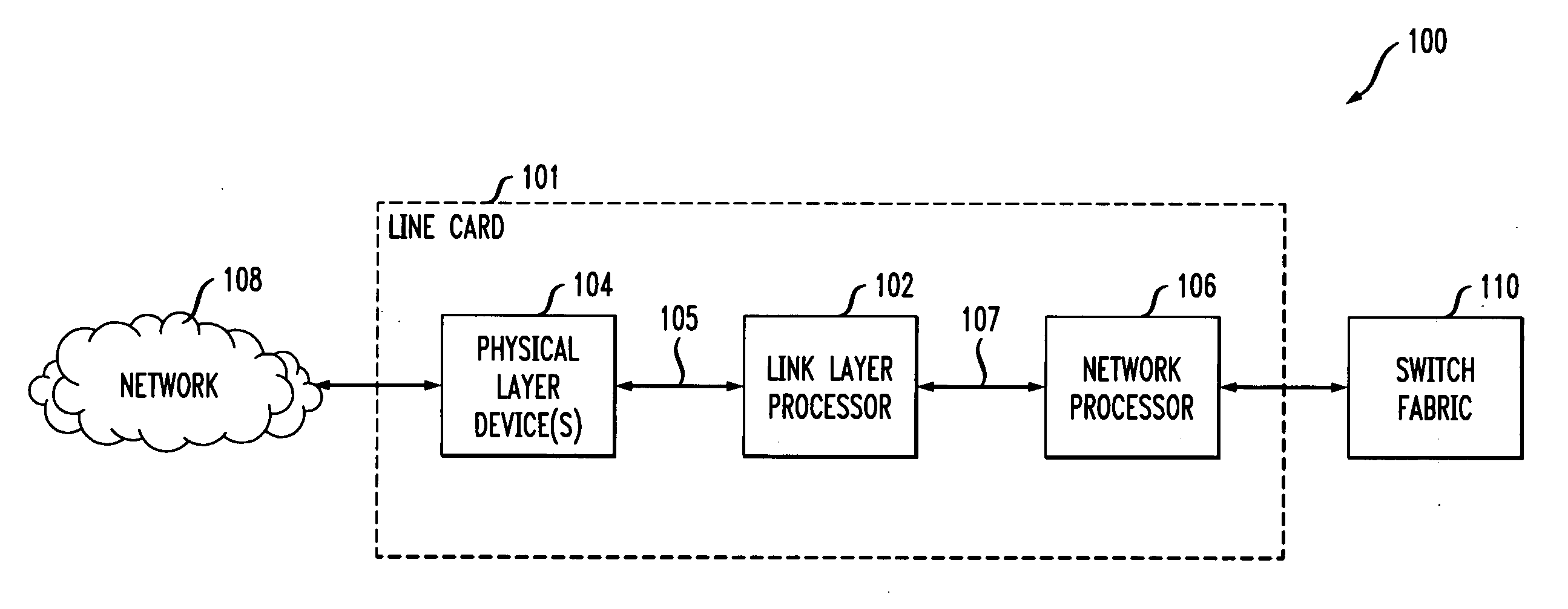
[0033]The invention will be illustrated herein in conjunction with an exemplary network-based communication system which includes a link layer device, a physical layer device and other elements configured in a particular manner. It should be understood, however, that the invention is more generally applicable to any system in which it is desirable to provide enhanced efficiency and flexibility in implementing digital PLLs in a link layer device so as to accommodate a variety of clock rates and clock transport mechanisms.

[0034]A “link layer device” as the term is used herein refers generally to a link layer processor or other type of processor which performs processing operations associated with a link layer of a network-based system. Such a device may be implemented, by way of example and without limitation, utilizing a microprocessor, central processing unit (CPU), digital signal processor (DSP), application-specific integrated circuit (ASIC), or other type of data processing devic...


PUM


Abstract

In a communication system comprising a link layer device connectable to one or more physical layer devices, the link layer device is configured using an efficient shared architecture for processing data associated with a plurality of links including at least one ingress link and at least one egress link. The link layer device comprises an ingress data clock processor configured to generate an ingress clock signal for processing data associated with said at least one ingress link, an egress data clock processor configured to generate an egress clock signal for processing data associated with said at least one egress link, and a control and configuration unit shared by the ingress data clock processor and the egress data clock processor. Another aspect of the invention relates to a buffer adaptive processor that in an illustrative embodiment limits clock variability in the presence of cell delay variation or cell loss.

Description

FIELD OF THE INVENTION[0001]The present invention relates generally to communication devices for use in network-based communication systems, and more particularly to clock processing in a link layer processor or other type of link layer device.BACKGROUND OF THE INVENTION[0002]A link layer processor is one example of what is more generally referred to herein as a link layer device, where the term “link layer” generally denotes a switching function layer. Such link layer devices can be used to implement processing associated with various packet-based protocols, such as Internet Protocol (IP) and Asynchronous Transfer Mode (ATM).[0003]Communication between a physical layer device and a link layer processor or other type of link layer device may be implemented in accordance with an interface standard, such as the SPI-3 interface standard described in Implementation Agreement OIF-SPI3-1.0, “System Packet Interface Level 3 (SPI-3): OC-48 System Interface for Physical and Link Layer Device...

Claims


Application Information

Patent Timeline
Patent Type & Authority Applications(United States)
IPC IPC(8): H04J3/06
CPCH04J3/0697H04L69/324
Inventor FRIEDMAN, ROBERTWAN, HONG
Owner INTEL CORP
Why Eureka
Try Eureka