De-embed method for multiple probes coupled to a device under test

a technology of multiple probes and devices, applied in liquid/fluent solid measurement, instruments, machines/engines, etc., can solve the problems of significant probe loading of circuits under test by probes, inaccurate representation of circuit voltages prior to probe loading, and inability to accurately represent circuit voltages. , to achieve the effect of reducing measurement errors

Inactive Publication Date: 2007-11-29
TEKTRONIX INC
View PDF31 Cites 33 Cited by
  • Summary
  • Abstract
  • Description
  • Claims
  • Application Information

AI Technical Summary

Benefits of technology

[0004]These and other deficiencies of the prior art are addressed by the present invention of a method for processing acquired time domain digital samples of a test signal from a device under test for reducing measurement errors due to, for example, loading of a device under test by multiple probes. Briefly, the invention provides a method to de-embed one or more probes and oscilloscope system so that loading and through effects of the probes and oscilloscope are substantially removed from the measurement. As a result, an equalization filter is generated for at least one of the probes coupled to the device under test such that the user will see a time domain display that represents the signal in a circuit under test as it would appear before the probes are attached to the circuit.

Problems solved by technology

This drop in impedance as frequency increases, coupled with the fact that many circuits being probed have a relatively low output impedance in the range of 25-150 ohms, results in a significant loading of the circuit under test by the probe.
As such, an acquired waveform received via a probe loading such a circuit may not accurately represent the voltage of the circuit prior to the introduction of the probe.
When more than one probe is coupled to the device under test, each probe may contribute to the loading of the device under test resulting in an inaccurate representation of the voltage of the circuit prior to the introduction of the probes.

Method used


Image

  • De-embed method for multiple probes coupled to a device under test
  • De-embed method for multiple probes coupled to a device under test
  • De-embed method for multiple probes coupled to a device under test

Examples


Embodiment Construction

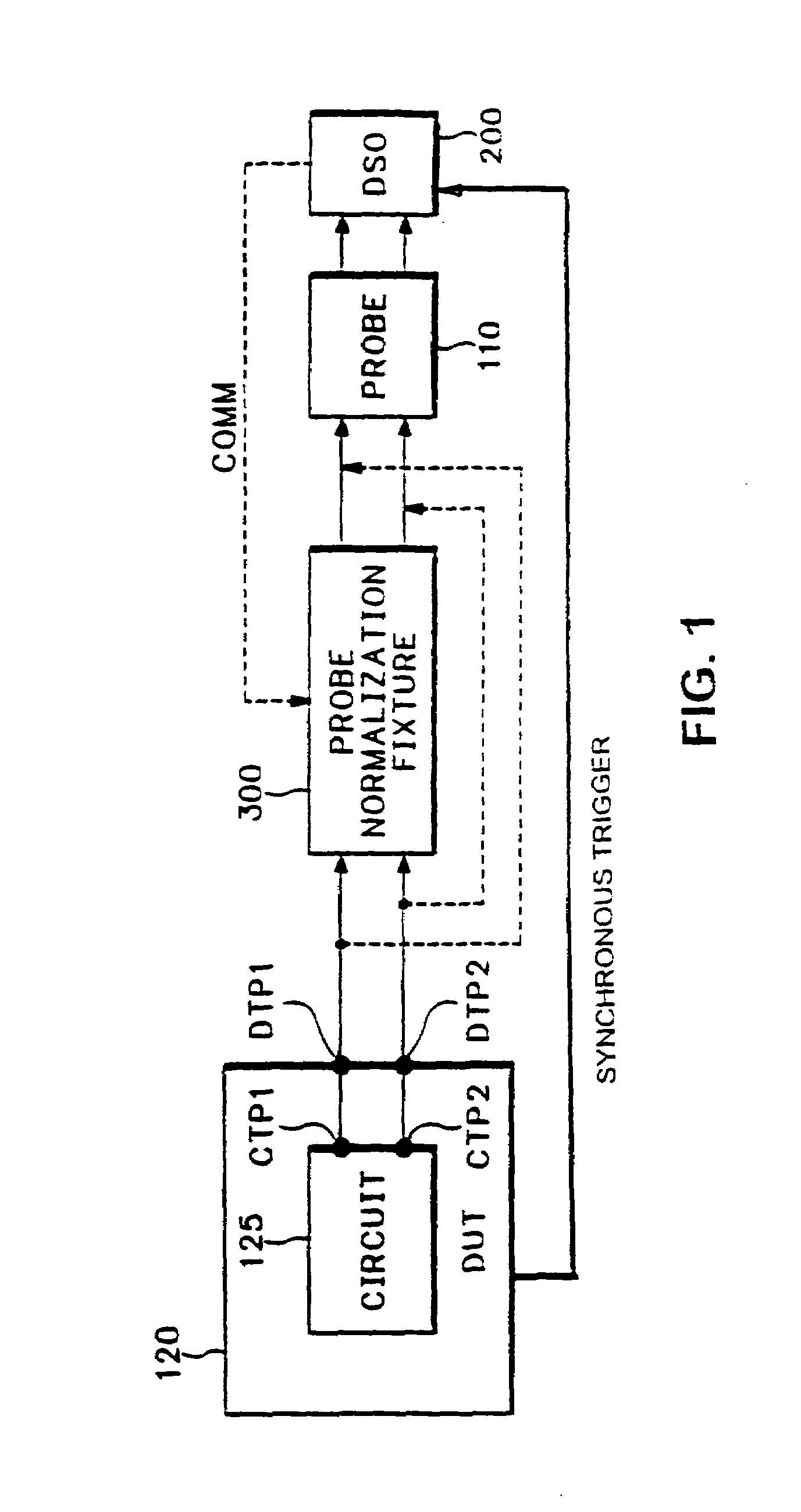
[0022]FIG. 1 depicts a high level block diagram of a testing system including a device under test arranged in accordance with an embodiment of the present invention. Specifically, a probe 110 is operably coupled to a signal analysis device such as a DSO 200 to provide thereto a signal under test (SUT) received from a device under test (DUT) 120. Interposed between the DUT 120 and the probe 110 is a probe normalization fixture 300.

[0023]In a calibrate mode of operation, the signal path between the DUT 120 and probe 110 passes through the probe normalization fixture 300. In a non-calibration mode of operation, a signal path between the DUT 120 and probe 110 is direct and excludes the probe normalization fixture 300. The calibration mode signal path is indicated by an unbroken line, while the non-calibration mode signal path is indicated by a dotted line. It will be noted that the probe paths depicted in FIG. 1 comprise two probe paths such as used within the context of a differential ...


PUM


Abstract

A method of de-embedding test probes coupled to an oscilloscope system to compensate for the loading of the test probes on a device under test. The method includes connecting each test probe individually to the device under test and calibrating each test probes to characterize transfer parameters of the device under test within a spectral domain. The open voltage of the device under test is calculated for each test probe. The test probes are connected to the device under test ans measurement samples are acquired by each of the test probes in the time domain and converted to the spectral domain. An equalization filter is computed for each of the test probes to compensate for loading of the device under test caused by the test probes using the spectral domain open voltage and measurement samples for each of the test probes.

Description

FIELD OF THE INVENTION[0001]The invention relates generally to signal acquisition systems and, more particularly, to a method for processing acquired digital samples of a test signal from device under test for reducing measurement errors due to, for example, probe tip loading of a device under test.BACKGROUND OF THE INVENTION[0002]Typical probes used for signal acquisition and analysis devices such as digital storage oscilloscopes (DSOs) and the like have an impedance associated with them which varies with frequency. For example, a typical probe may have an impedance of 100K to 200K Ohms at DC, which impedance drops towards 200 ohms at 1.5 GHz. Higher bandwidth probes drop to even lower impedance values. This drop in impedance as frequency increases, coupled with the fact that many circuits being probed have a relatively low output impedance in the range of 25-150 ohms, results in a significant loading of the circuit under test by the probe. As such, an acquired waveform received vi...

Claims


Application Information

Patent Timeline
Patent Type & Authority Applications(United States)
IPC IPC(8): G06F19/00
CPCG01R35/00G01R27/32
Inventor TAN, KANPICKERD, JOHN J.
Owner TEKTRONIX INC
Why Eureka
Try Eureka