Structure and a method for monolithic integration of HBT, depletion-mode HEMT and enhancement-mode HEMT on the same substrate

a technology of hemt and hbt, which is applied in the direction of basic electric elements, electrical equipment, semiconductor devices, etc., can solve the problems of limited ability of current semiconductor fabrication techniques, and achieve the effect of facilitating monolithic integration of hb

Inactive Publication Date: 2007-12-06
WIN SEMICON
View PDF3 Cites 43 Cited by
  • Summary
  • Abstract
  • Description
  • Claims
  • Application Information

AI Technical Summary

Benefits of technology

[0004]It is an object of the present invention to provide a stacked-layer structure containing HBT layers on the

Problems solved by technology

However, HBT devices are known to be handicapped with high turn-on voltage, leading to an undesirable high reference voltage in power amplifiers, which is not favorab

Method used


Image

  • Structure and a method for monolithic integration of HBT, depletion-mode HEMT and enhancement-mode HEMT on the same substrate
  • Structure and a method for monolithic integration of HBT, depletion-mode HEMT and enhancement-mode HEMT on the same substrate
  • Structure and a method for monolithic integration of HBT, depletion-mode HEMT and enhancement-mode HEMT on the same substrate

Examples


Embodiment Construction

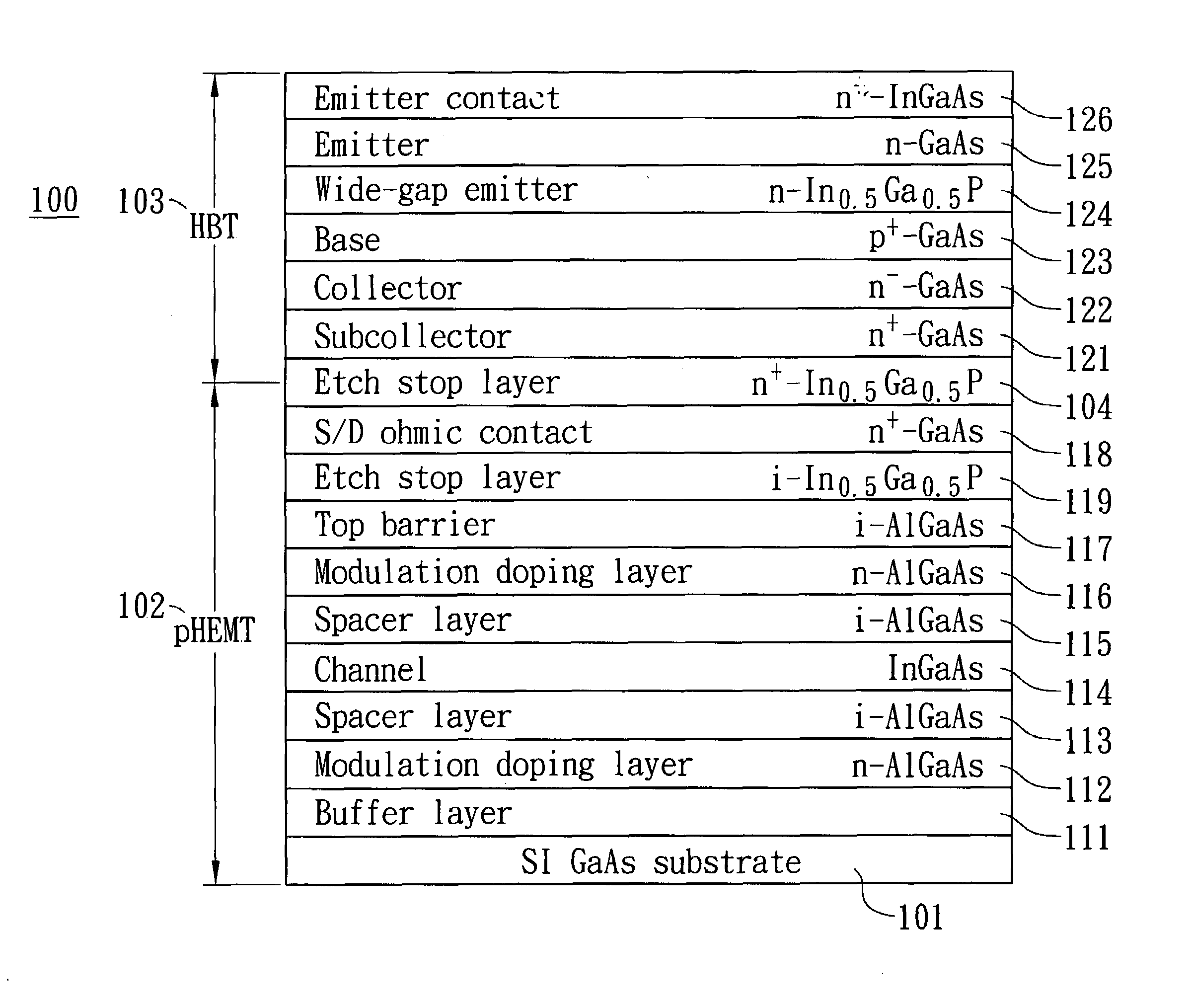
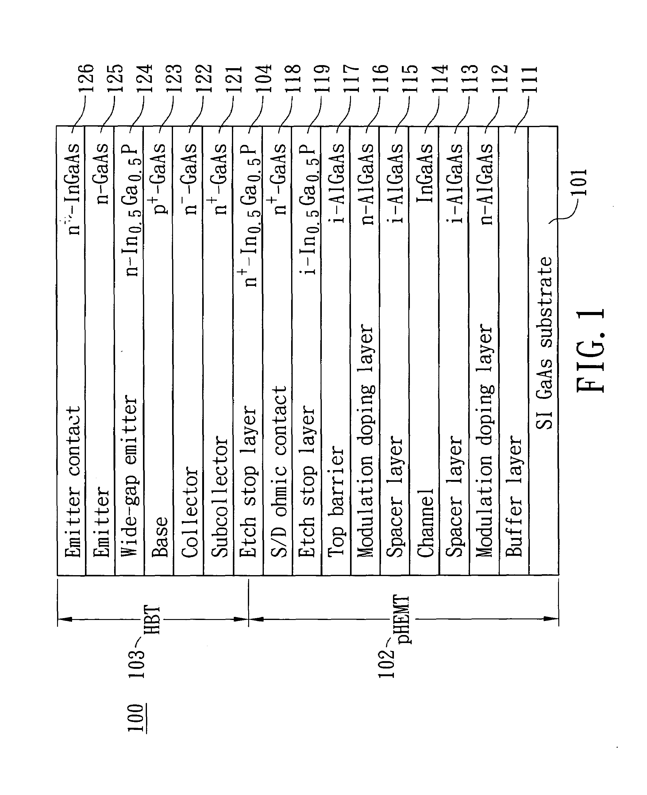
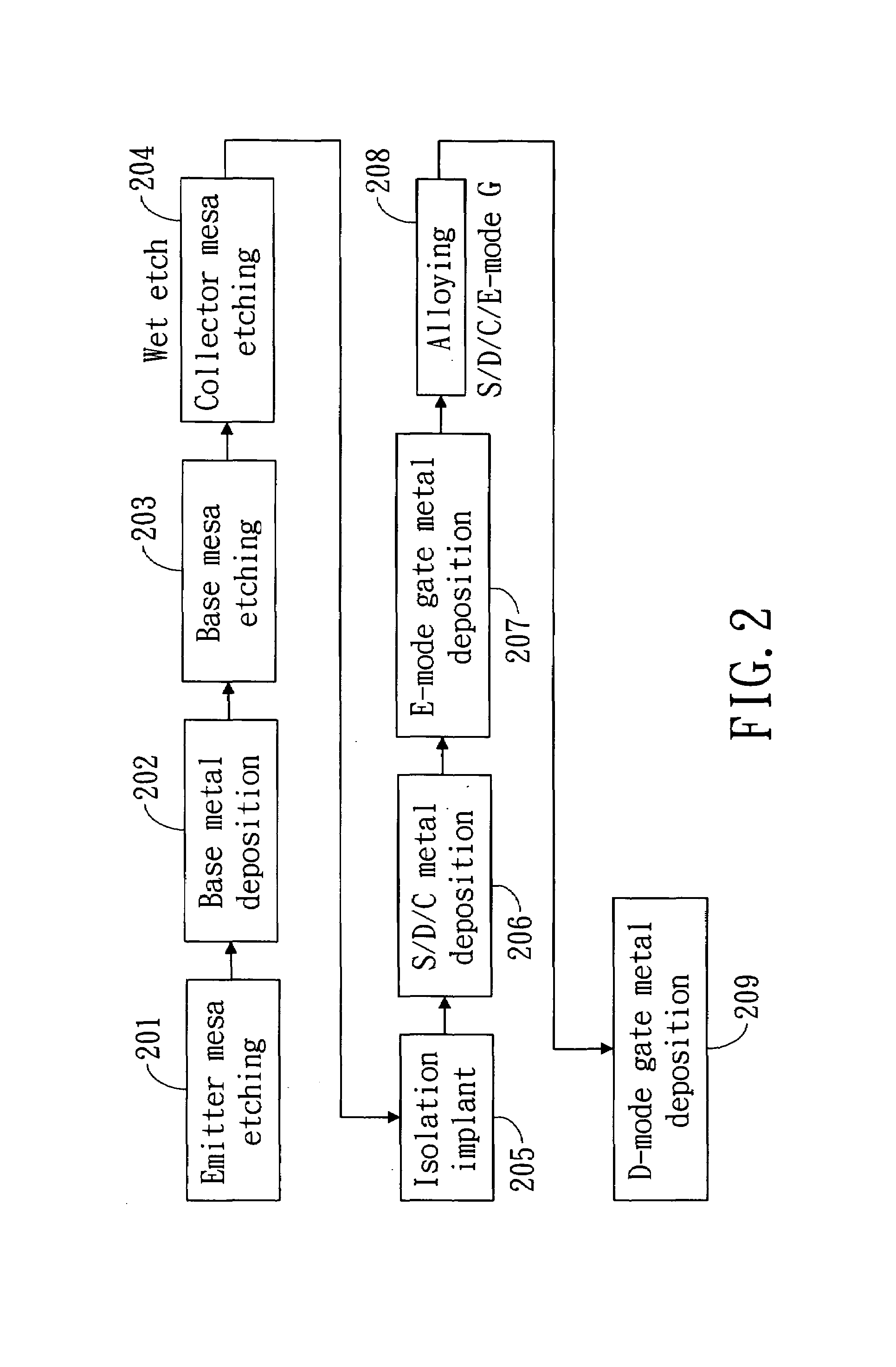
[0018]FIG. 1 illustrates the epitaxial layer structure used for the invention 100. It is basically a vertically stacked-layer structure, which generally consists of HEMT layers with HBT layers thereon, formed on a substrate 101. The substrate is preferably a semi-insulating GaAs substrate, or other suitable substrates for epitaxial growth of the stacked-layer structure thereon. After providing the substrate 101, the stacked-layer structure are then grown on the substrate 101 by well-known technologies, such as molecular beam epitaxy (MBE), or metalorganic chemical vapor deposition (MOCVD). The stacked-layer structure generally consists of two set of layers: the first set of layers is the HEMT layers 102, and the second set is the HBT layers 103. An etching stop layer 104, which may be an InGaP layer, is inserted between these two sets of layers in order to facilitate the fabrication processes for the HBT and the HEMT devices.

[0019]As a embodiment of the invention, the HEMT layers 10...


PUM


Abstract

An epitaxial layers structure and a method for fabricating HBTs and HEMTs on a common substrate are disclosed. The epitaxial layers comprise generally a set of HBT layers on the top of a set of HEMT layers. The method can be used to fabricate HBT, E-mode HEMT and D-mode HEMT as well as passive devices, that enabling monolithic integration of a significant number of devices on a common substrate by a cost-effective way.

Description

FIELD OF THE INVENTION[0001]The present invention relates in general to integrated circuits made of III-V compound semiconductors and, in particular, to a stacked-layer structure containing HBT layers on the top of HEMT layers, and to a method for fabricating HBTs, depletion-mode pHEMTs, enhancement-mode pHEMTs as well as passive devices, that enables monolithic integration of a significant number of devices on a common substrate.BACKGROUND OF THE INVENTION[0002]Integration of multifunction circuit devices, which include more than one device type on a common substrate, in certain applications (such as microwave, millimeter wave, and optoelectronic application) not only increases the performance of the integrated circuits, but also provides a practical solution to achieve greater cost and space reduction. For example, by integrating heterojunction bipolar transistors (HBTs) and heterojunction field-effect transistors (HFETs), such as high-electron-mobility transistors (HEMTs) in gene...

Claims


Application Information

Patent Timeline
IPC IPC(8): H01L29/739
CPCH01L21/8252H01L27/0605H01L29/7785H01L29/66462H01L29/7371H01L29/66318
Inventor LIN, HENG-KUANGCHAO, CHIA-LIANGTU, MING-CHANGTSAI, TSUNG-CHIWANG, YU-CHI
Owner WIN SEMICON
Why Eureka
Try Eureka