MEMS device and method of fabricating the same

Active Publication Date: 2007-12-06
AKUSTICA
View PDF19 Cites 48 Cited by
  • Summary
  • Abstract
  • Description
  • Claims
  • Application Information

AI Technical Summary

Benefits of technology

[0007]An object of the present invention is to provide a MEMS device tha

Problems solved by technology

Currently, present fabrication processing is inefficient and costly due to th

Method used


Image

  • MEMS device and method of fabricating the same
  • MEMS device and method of fabricating the same
  • MEMS device and method of fabricating the same

Examples


Embodiment Construction

[0019]Reference will now be made in detail to the preferred embodiments of the present invention, examples of which are illustrated in the accompanying drawings.

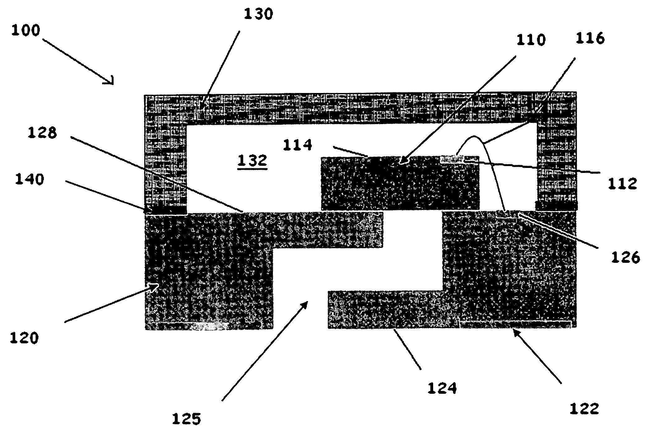
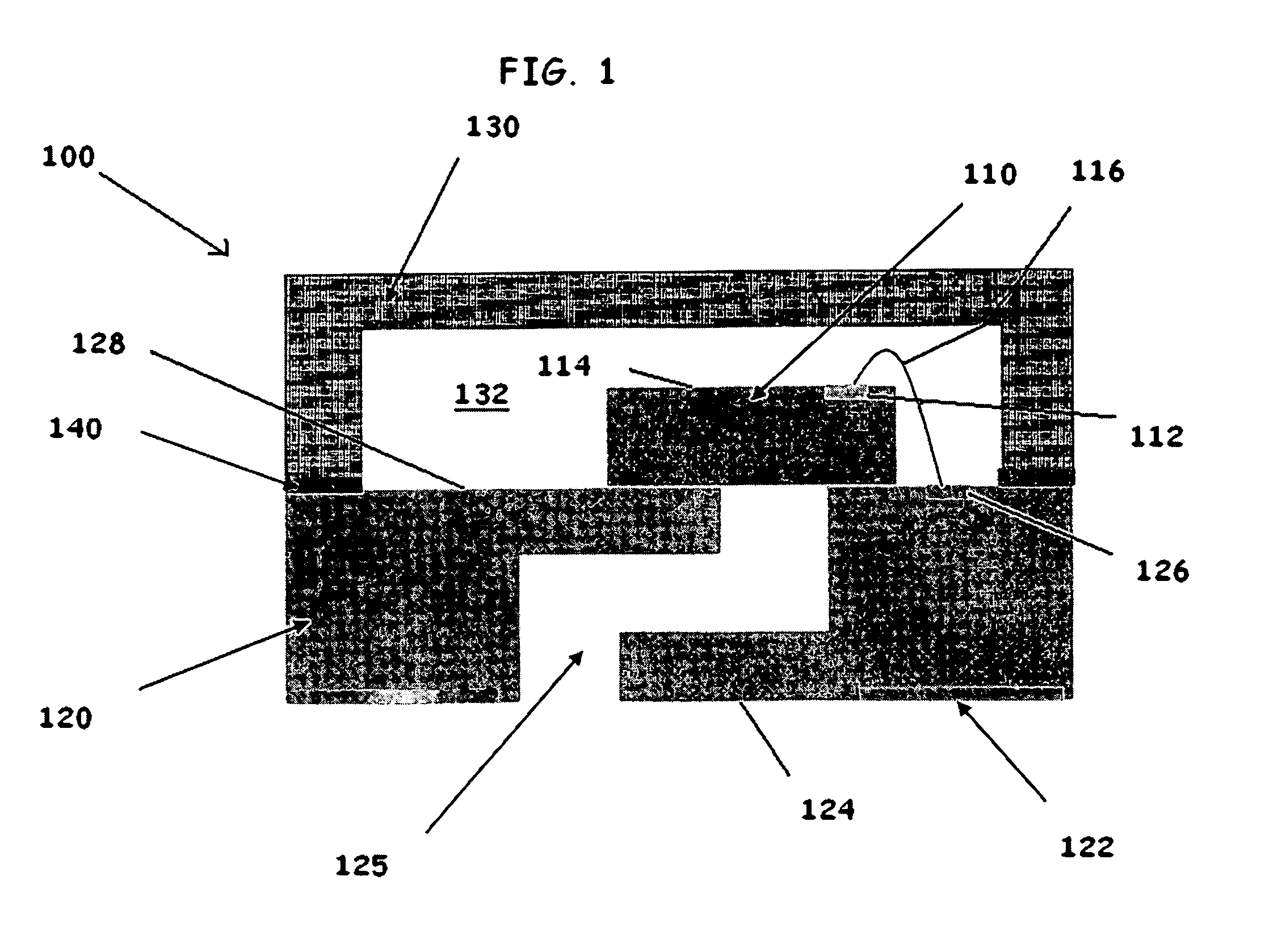
[0020]FIG. 1 is a schematic side view of an exemplary MEMS device according to the present invention. In FIG. 1, a MEMS device 100 may include a MEMS die 110 mounted onto a chip carrier 120 that is encapsulated by an enclosure 130. The enclosure 130 may be formed as a molded single piece enclosure that is isotropically electrically conductive. Accordingly, the enclosure 130 may be bonded to the chip carrier 120 using an adhesive bond 140 along a periphery of the chip carrier 120 to seal an interior region 132 of the enclosure 130 from an exterior of the MEMS device 100. The adhesive bond 140 may include an electrically conductive material, such as a paste, supporting film, or tape, in order to provide for an electrical interconnection between the electrically conductive enclosure 130 and the chip carrier 120.

[0021]In FIG. 1,...


PUM


Abstract

A MEMS device includes a chip carrier having an acoustic port extending from a first surface to a second surface of the chip carrier, a MEMS die disposed on the chip carrier to cover the acoustic port at the first surface of the chip carrier, and an enclosure bonded to the chip carrier and encapsulating the MEMS die.

Description

BACKGROUND OF THE INVENTION[0001]1. Field of the Invention[0002]The present invention relates to a micro-electro-mechanical system (MEMS) device and a method of fabricating the same.[0003]2. Discussion of the Related Art[0004]In general, micro-electro-mechanical system (MEMS) devices are the integration of mechanical elements, such as sensors, actuators, and electronics, on a common silicon substrate using integrated circuit (IC) processes. For example, micromechanical components are fabricated using processes that selectively etch away parts of the silicon wafer or add new structural layers to form the mechanical and / or electromechanical devices.[0005]The fabrication of MEMS devices allows for on-chip devices that include both microsensors and microactuators, as well as control systems to operate the microactuators and receive information from the microsensors. However, MEMS devices require encapsulation to prevent external interference with the functions of the microsensors and mi...

Claims


Application Information

Patent Timeline
IPC IPC(8): H01L29/84
CPCB81B2201/0257B81B2207/096H01L2924/1461H01L2924/10253H01L2224/48091H04R31/006H04R19/016B81C1/00333B81C2203/0109H04R1/04H01L2924/00014H01L2924/00B81B7/02B81C1/00H01L29/84
Inventor GOODELLE, JASON P.GABRIEL, KAIGHAM J.
Owner AKUSTICA
Why Eureka
Try Eureka