Solid-state imaging device, method of driving the same, and camera

Inactive Publication Date: 2007-12-06
SONY SEMICON SOLUTIONS CORP
View PDF11 Cites 28 Cited by
  • Summary
  • Abstract
  • Description
  • Claims
  • Application Information

AI Technical Summary

Benefits of technology

[0027] In the column-parallel analog-to-digital conversion at the solid-state imaging device, it is possible to reduce a conversion time to approximately 2m order in the case of the uppermost m bits and to approximately 2n−m order in the case of the lowermost (n−m) bits by separately performing the uppermost m-bit analog-to-digital conversion from the lowermost (n−m) -bit analog-to-digital conversion. Therefore, it is also possible to moderate the element accuracy.
[0028] Further, in the column-parallel analog-to-digital conversion at the solid-state imaging device, the counter-ramp-type analog-to-

Problems solved by technology

However, the counter-ramp-type analog-to-digital converter using the single slope shown in FIG. 8 has a problem that the conversion time should be increased or a clock frequency should be increased in order to improve the accuracy of the analog-to-digital conversion.
When the conversion time is about two times longer, it is difficult to implement a high speed operation such as the high frame rate of the solid-state imaging device or high pixilati

Method used


Image

  • Solid-state imaging device, method of driving the same, and camera
  • Solid-state imaging device, method of driving the same, and camera
  • Solid-state imaging device, method of driving the same, and camera

Examples


Embodiment Construction

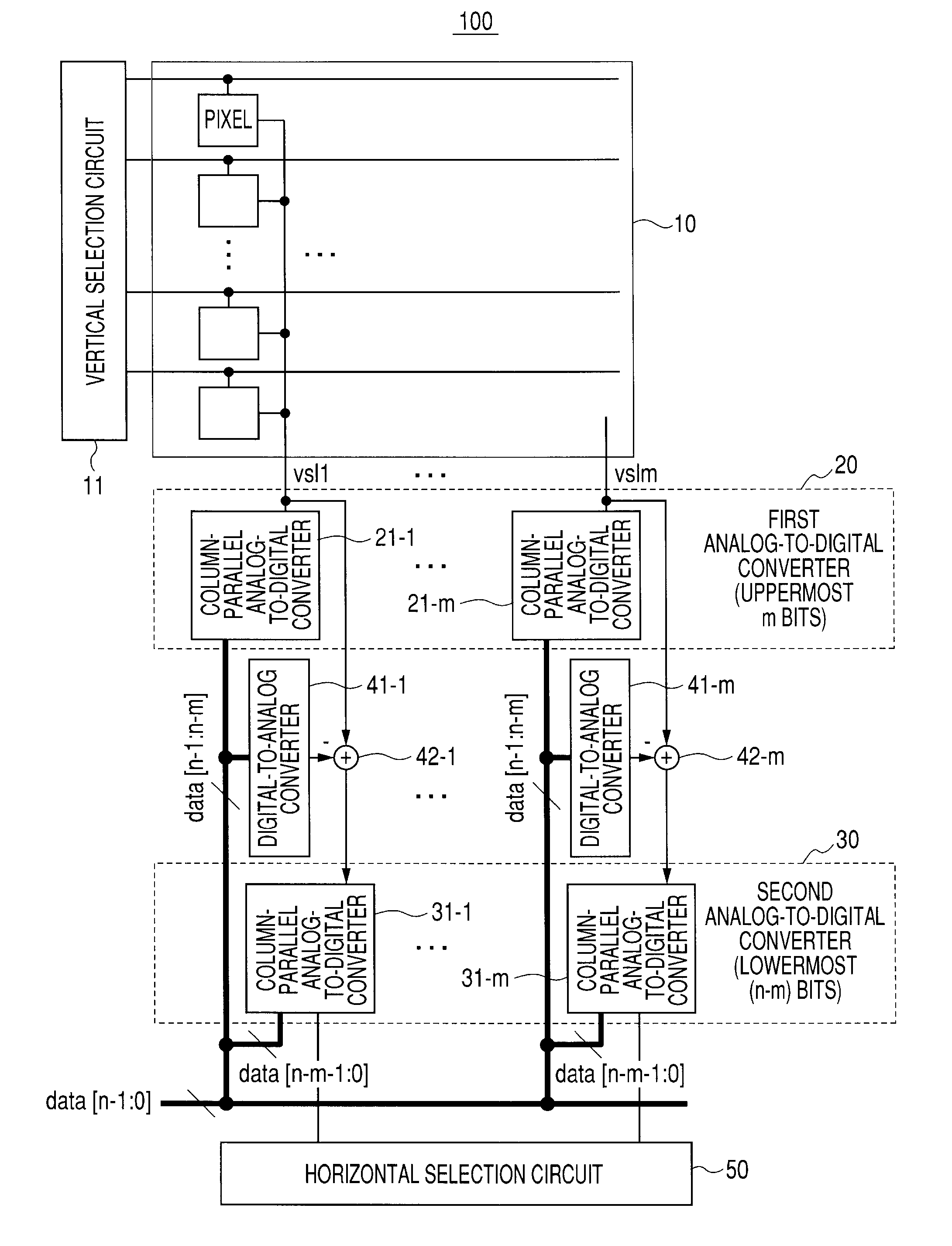
[0041]FIG. 1 is a diagram illustrating the block structure of a solid-state imaging device 100 including a column-parallel analog-to-digital converter according to an embodiment of the invention.

[0042] The solid-state imaging device 100 includes a pixel unit 10 which will be described later, a first uppermost m-bit analog-to-digital converter 20, a second lowermost (n−m)-bit analog-to-digital converter 30 (where, m and n are arbitrary positive integers and n is larger than m), a timing signal generator (not shown), a vertical selection circuit 11, and a horizontal selection circuit 50.

[0043] The timing signal generator (not shown) receives a vertical synchronization signal, a horizontal synchronization signal, a sensor driving clock, and a sensor reset signal from the external of a sensor of the solid-state imaging device 100. The timing signal generator generates a timing signal so as to drive the vertical selection circuit 11, the horizontal selection circuit 50, the column-para...


PUM


Abstract

A solid-state imaging device includes: a plurality of pixels which are arranged in a matrix; a sequential scanning device that selects each row of pixels; and an analog-to-digital conversion unit having a first analog-to-digital converter that is connected to a vertical signal line to which a pixel signal is supplied from the pixel and performs a first bit-length analog-to-digital conversion on an output signal from the vertical signal line or a pixel output signal obtained by sampling the output signal, and a second analog-to-digital converter that, when the first analog-to-digital converter completes the conversion operation, subtracts an analog signal corresponding to the first bit-length from the pixel output signal and then performs a second bit-length analog-to-digital conversion.

Description

CROSS REFERENCES TO RELATED APPLICATIONS [0001] The present invention contains subject matter related to Japanese Patent Application JP 2006-059857 filed in the Japanese Patent Office on Mar. 6, 2006, the entire contents of which being incorporated herein by reference. BACKGROUND OF THE INVENTION [0002] 1. Field of the Invention [0003] The invention relates to a solid-state imaging device including column-parallel analog-to-digital converters provided to outputs of a plurality of vertical signal lines and capable of moderating device accuracy and reducing a conversion time, to a method of driving the solid-state imaging device, and to a camera. [0004] 2. Description of the Related Art As shown in FIG. 8, a known solid-state imaging device 400 including a column-parallel analog-to-digital converter generally uses a counter-ramp-type analog-to-digital converter using a single slope. [0005] The operation of the analog-to-digital converter shown in FIG. 8 will be described with referenc...

Claims


Application Information

Patent Timeline
IPC IPC(8): H04N3/14H01L27/146H03M1/14H03M1/56H04N5/335H04N5/369H04N5/374H04N5/378
CPCH03M1/145H04N5/378H04N5/335H04N25/00H04N25/75H04N25/77
Inventor SATO, HIROKI
Owner SONY SEMICON SOLUTIONS CORP
Why Eureka
Try Eureka