Liquid crystal device and electronic apparatus

a technology of electronic equipment and liquid crystal, which is applied in the direction of instruments, non-linear optics, optics, etc., can solve the problems of narrow viewing angle, and achieve the effect of increasing brightness

Inactive Publication Date: 2007-12-06
EPSON IMAGING DEVICES CORP
View PDF29 Cites 28 Cited by
  • Summary
  • Abstract
  • Description
  • Claims
  • Application Information

AI Technical Summary

Benefits of technology

[0007]An advantage of some aspects of the invention is that it provides a liquid crystal device in the FFS mode, which is capable of performing a display operation with a higher brightness, and an electronic apparatus including the same.

Problems solved by technology

In known liquid crystal devices using twisted nematic (TN) liquid crystal, the narrow viewing angle has been regarded as a problem.

Method used


Image

  • Liquid crystal device and electronic apparatus
  • Liquid crystal device and electronic apparatus
  • Liquid crystal device and electronic apparatus

Examples


first embodiment

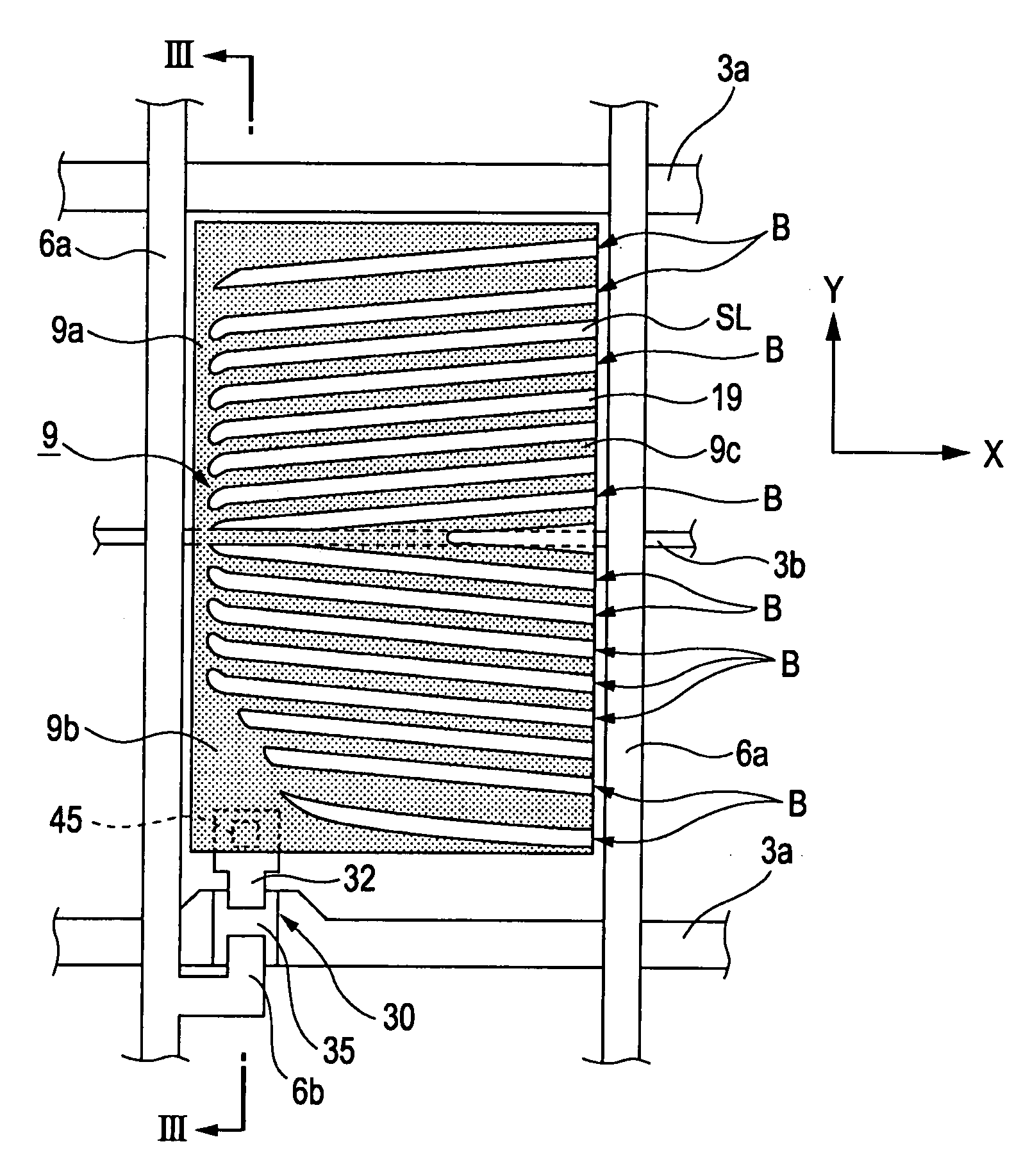
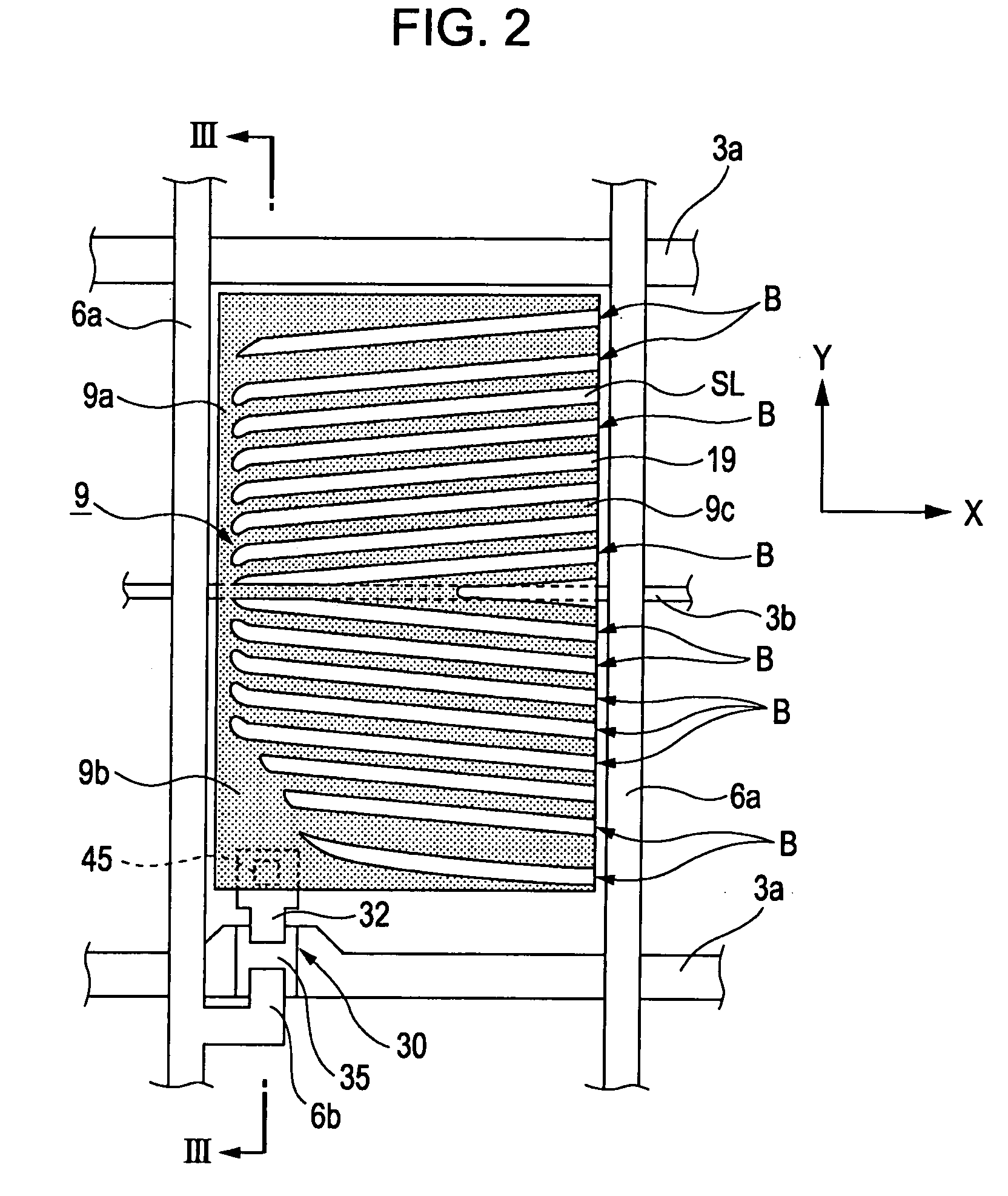
[0034]A liquid crystal device according to a first embodiment of the invention will be described with reference to the drawings. The liquid crystal device according to the first embodiment is a liquid crystal device in the FFS mode. The FFS mode is one of horizontal electric field modes in which an image is displayed by applying an electric field (horizontal electric field) to liquid crystal in a direction of the surface of each substrate to control the alignment of the liquid crystal.

[0035]The liquid crystal device according to the first embodiment is a color liquid crystal device having color filters on the substrate. One pixel has three subpixels emitting red (R), green (G), and blue (B) light beams, respectively. A display region serving as the minimum unit constituting an image display region is referred to as a “subpixel region”, and a display region including a set of subpixels (R, G, and B) is referred to as a “pixel display region”.

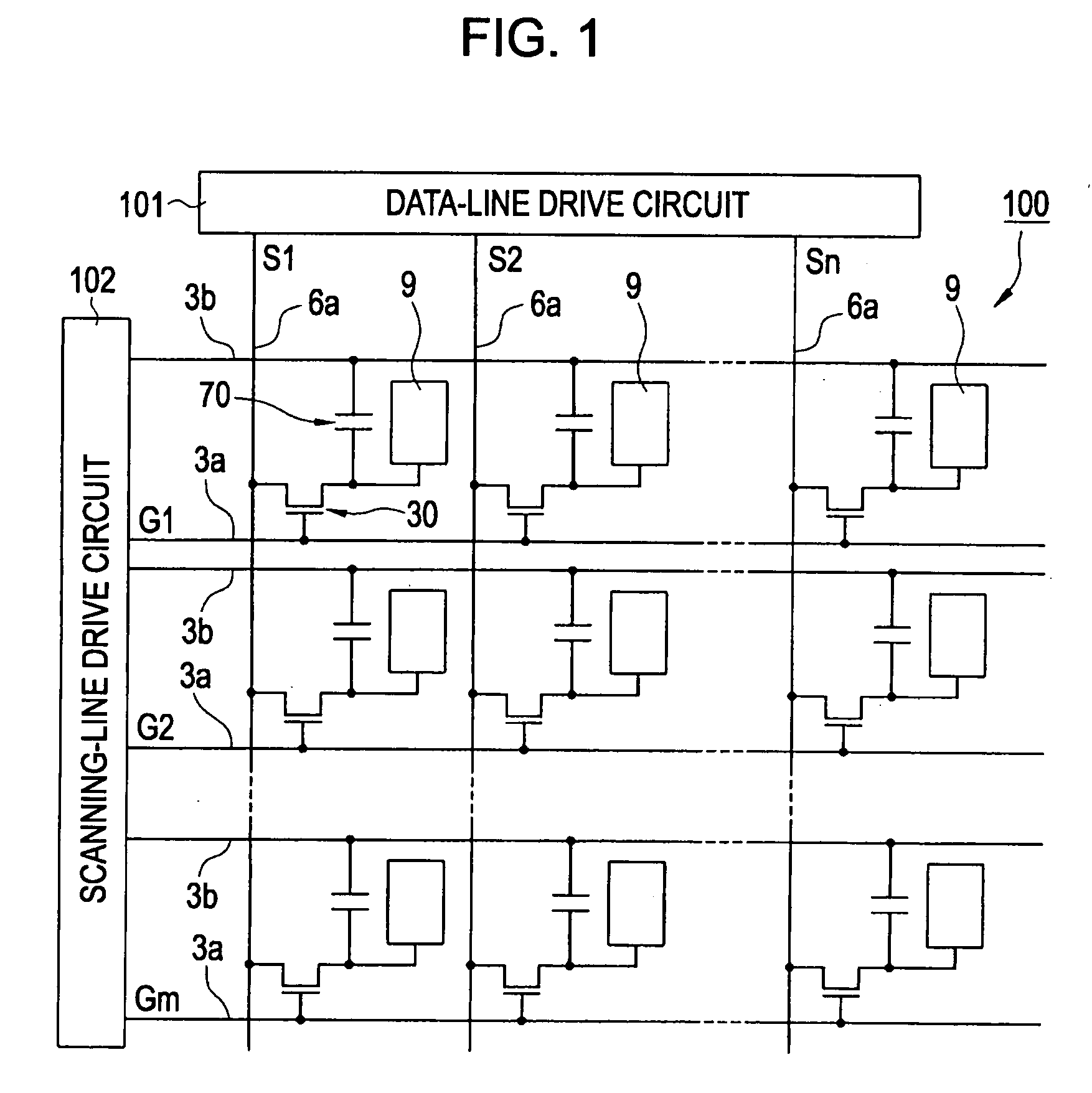
[0036]FIG. 1 is a circuit diagram showing ...

second embodiment

[0097]A second embodiment of the invention will be described with reference to the drawing.

[0098]A liquid crystal device according to the second embodiment differs from those described in the first embodiment and the modification in that a backbone portion 209a that connects multiple strip electrodes 209c with one another covers two ends of the adjacent strip electrodes 209c. The components of the liquid crystal device according to the second embodiment, that is, the liquid crystal layer 50, the TFT array substrate 10, the counter substrate 20, the polarizing plates 14 and 24, and the like, are the same as those of the first embodiment. In the following description, descriptions of portions common to the first embodiment and the modification are omitted.

[0099]FIG. 8 is a plan view showing the structure of one subpixel region of the liquid crystal device according to the second embodiment. FIG. 8 corresponds to FIG. 2 showing the first embodiment.

[0100]In the liquid crystal device ac...


PUM

PropertyMeasurementUnit
positional displacementaaaaaaaaaa
angleaaaaaaaaaa
angleaaaaaaaaaa

Abstract

A liquid crystal device includes a first substrate and a second substrate facing each other with a liquid crystal layer held therebetween; first electrodes and second electrodes provided on a surface of the first substrate, the surface facing toward the liquid crystal layer; data lines and scanning lines provided on the surface of the first substrate, the surface facing toward the liquid crystal layer, the data lines and the scanning lines intersecting one another; and switching elements connected to the corresponding data lines and the corresponding scanning lines. The alignment of liquid crystal molecules of the liquid crystal layer is controlled by an electric field induced between the first and second electrodes. The first electrodes are arranged in corresponding pixel regions enclosed by the data lines and the scanning lines. Each of the second electrodes has a plurality of branch electrodes extending in a direction intersecting a corresponding one of the data lines and a connecting portion electrically connecting the branch electrodes with one another such that at least one of first and second ends of the adjacent branch electrodes is open. The second electrodes are arranged such that each of the second electrodes partially overlaps a corresponding one of the first electrodes in a corresponding one of the pixel regions when viewed in plan.

Description

BACKGROUND[0001]1. Technical Field[0002]The present invention relates to liquid crystal devices and electronic apparatuses.[0003]2. Related Art[0004]In known liquid crystal devices using twisted nematic (TN) liquid crystal, the narrow viewing angle has been regarded as a problem. To solve this problem, liquid crystal devices in the fringe field switching (FFS) mode have been proposed. In such a liquid crystal device in the FFS mode, first electrodes and second electrodes are arranged on one of a pair of substrates sandwiching a liquid crystal layer, and the liquid crystal layer is driven by an electric field (horizontal electric field) induced between the first and second electrodes.[0005]JP-A-2002-182230 discloses a liquid crystal device in the FFS mode in which color shift and disclination are prevented from occurring by forming rectangular apertures tilted at a predetermined angle in each of the second electrodes or pixel electrodes.[0006]In the liquid crystal device described in...

Claims


Application Information

Patent Timeline
Patent Type & Authority Applications(United States)
IPC IPC(8): G02F1/1343
CPCG02F2001/134372G02F1/134363G02F1/134372G02F1/1343
Inventor MATSUSHIMA, TOSHIHARU
Owner EPSON IMAGING DEVICES CORP
Why Eureka
Try Eureka