Memory device, memory system and method of operating such

a memory device and memory technology, applied in the direction of information storage, static storage, digital storage, etc., can solve the problems of inability to produce identical devices, individual devices are subject to process-related variances, and the demand for memory capacity cannot be fulfilled by a single device, so as to prevent collisions and prevent too little loading of signal paths

Inactive Publication Date: 2007-12-06
POLARIS INNOVATIONS
View PDF5 Cites 11 Cited by
  • Summary
  • Abstract
  • Description
  • Claims
  • Application Information

AI Technical Summary

Benefits of technology

[0049] According to an embodiment of the present invention, the method additionally comprises a conversion of the latency period into a set of data or into a set of serial binary data. The latency period determined, e.g. in the form of a count reached within the latency period, can thus be forwarded in the form of normal data via the data path or also forwarded to a further output, e.g. in the form of serial data, in a simple manner and with minimum wiring expenditure, for example to a memory controller for determining a maximum latency period.
[0050] According to an embodiment of the present invention, the method comprises an insertion of the data read out of the at least two memory devices into a common data stream. The common data stream, for example in the form of a common signal path can thus be utilized by a number of memory devices. The data can be inserted with bit accuracy so that both collisions and too little loading of the signal paths is prevented.

Problems solved by technology

Often, however, memory capacities are demanded which cannot be fulfilled by a single device.
In spite of the high and optimized reproducibility of established production processes, it is impossible to produce identical devices.
Instead, the individual devices are subject to process-related variances which become noticeable mainly with regard to a latency period varying from device to device.
Furthermore, fluctuations in the supply voltage and the ambient temperature during the operation also lead to a change in latency period.
Otherwise, collisions occur when a memory device outputs data at a time at which data signals are already present at the location of the signal entry.
Furthermore, too generous a waiting time between two successive read requests can lead to inadequate loading of the signal path.

Method used


Image

  • Memory device, memory system and method of operating such
  • Memory device, memory system and method of operating such
  • Memory device, memory system and method of operating such

Examples


first embodiment

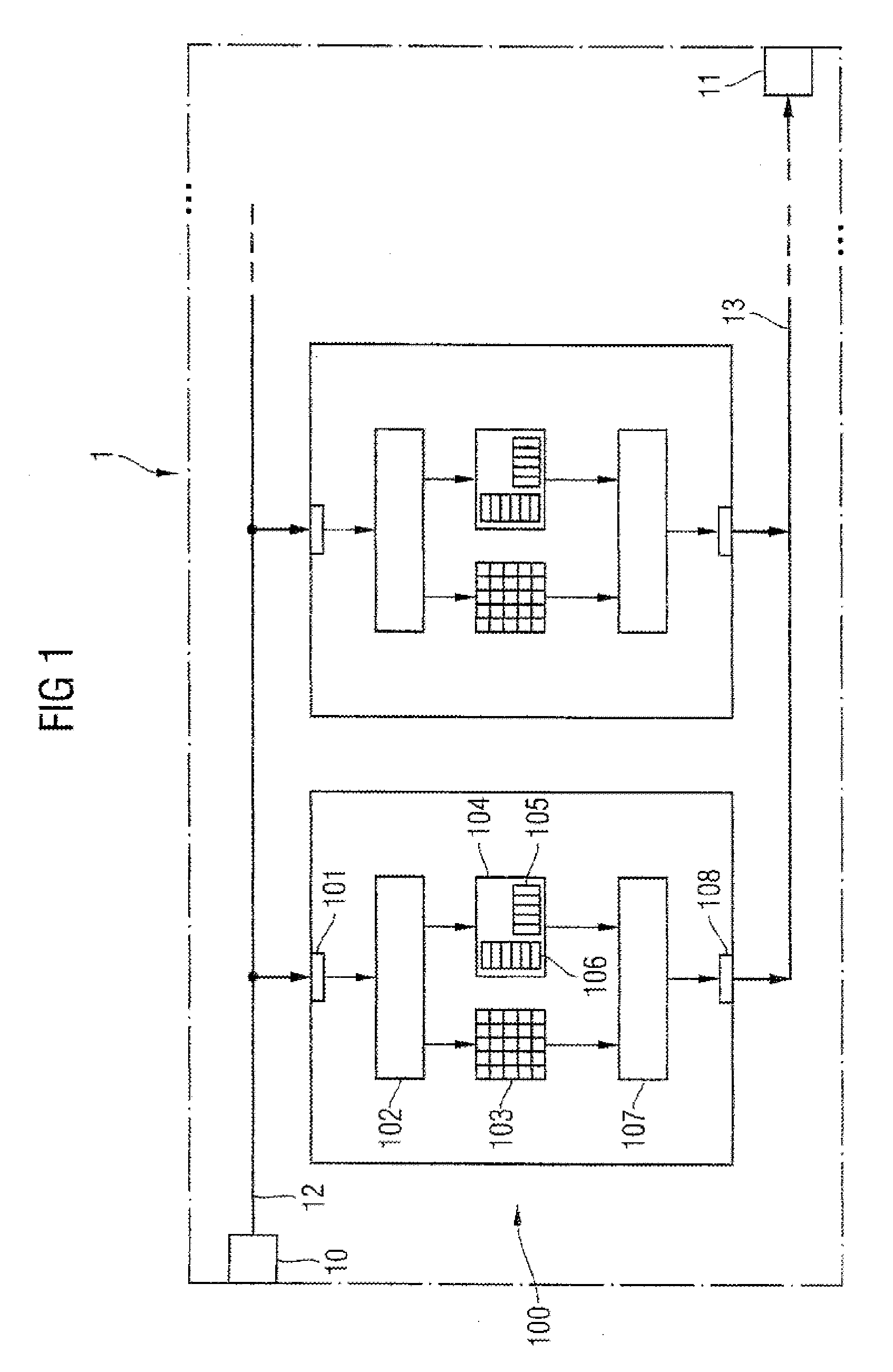
[0064]FIG. 1 shows a diagrammatic representation of a memory module 1 comprising at least two first memory devices 100. The memory module 1 receives command data, e.g. from a memory controller or a microprocessor, via a command data input 10. The command data are forwarded from the command data input 10 via a first signal line 12 to the memory devices 100. According to this first embodiment of the present invention, any form of parallel circuit is provided. As shown here, the first signal line 12 may comprise branches to the first inputs 101 of the memory devices 100. The command data thus reach the first input 101 and are forwarded to the input circuit 102 within a memory device 100. The input circuit 102 provides drive signals for a memory cell array 103 and a timer 104. The memory cell array 103 outputs data in dependence on drive signals provided to it and provides them to the output buffer 107.

[0065] The timer 104 drives the output buffer 107 in such a manner that it outputs th...

second embodiment

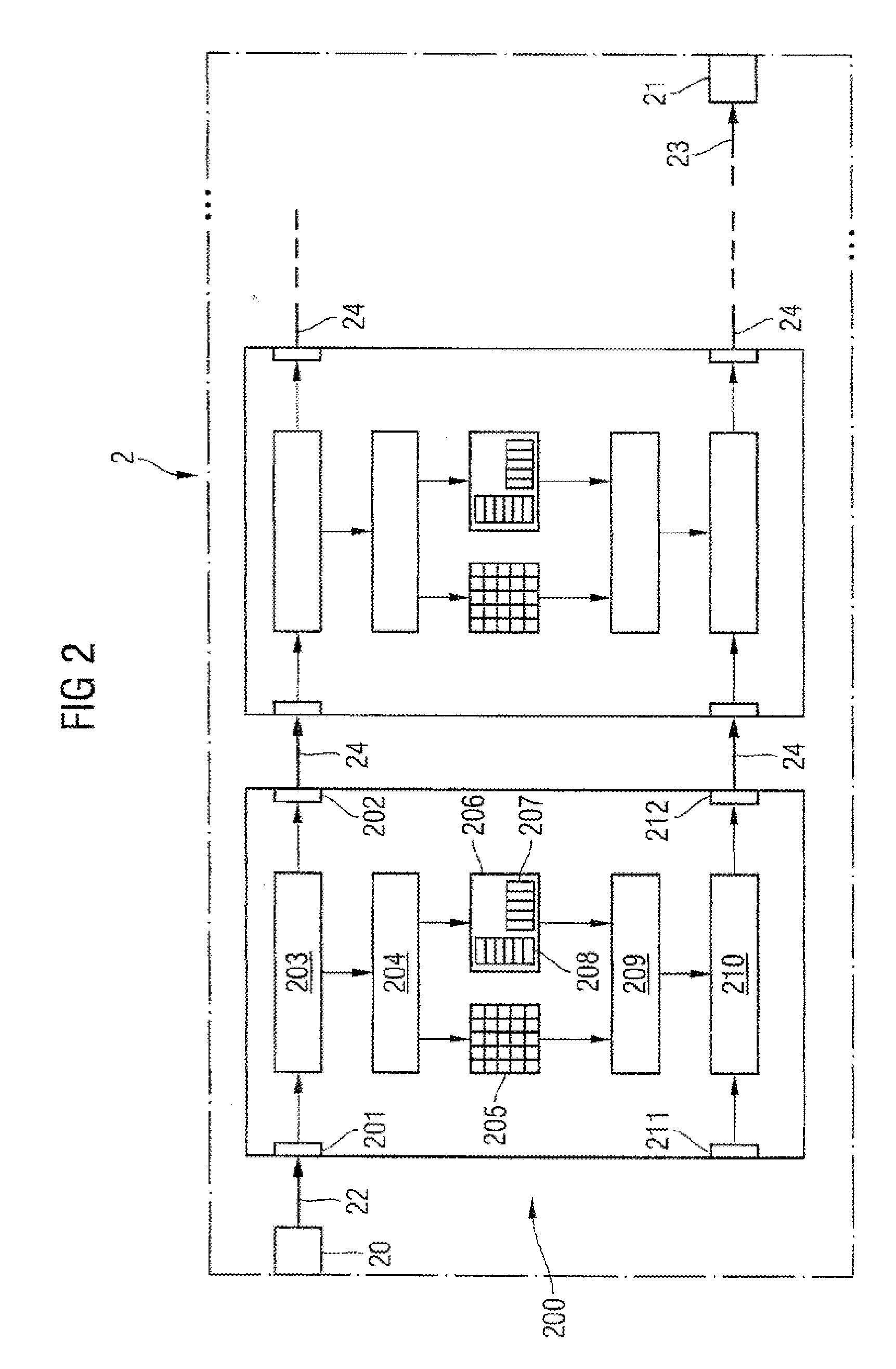
[0067]FIG. 2 shows a diagrammatic representation of a memory module 2 according to the present invention. The memory module 2 comprises at least two memory devices 200. A memory device 200 has a first input 201, a first transfer unit 203 and a second output 202 for receiving command data and for forwarding the command data. The transfer unit 203 correspondingly forwards the command data to the second output 202 and / or to the input circuit 204.

[0068] Drive signals are provided by the input circuit 204 to a memory cell array 205 and a timer 206. The timer has a register 207 and a counting unit 208 in order to drive an output buffer 209 in such a manner that it outputs the data read out of the memory cell array 205 after the expiry of an adjustable time interval after the provision of the drive signals. The register 207 and the counting unit 208 which counts clock cycles of a clock signal are used for determining the adjustable time interval and its expiry.

[0069] The memory device 200...

third embodiment

[0072]FIG. 3 shows a diagrammatic representation of a memory module 3 according to the present invention. Analogously to the preceding embodiment, the memory module 3 comprises a command data input 30 and a first signal line 32 for forwarding command data from, for example, a memory controller or microprocessor to memory devices 300 of the memory module 3. The data read out of the memory devices 300 are forwarded to a data output 31 of the memory module 3 by a second signal line 33. A module signal line system 34 forwards both the command data and the data read out between the memory devices 300. The memory devices 300 comprise a first input 301, a first transfer unit 303, a second output 302, a second input 314, a second transfer unit 313, and a first output 315 for the through-conduction of the command data and the data read out. The command data forwarded by the first transfer unit 303 to an input circuit 304 are used for providing drive signals for the memory cell array 305, a t...


PUM


Abstract

A memory device comprising a memory cell array; an input circuit providing drive signals to the memory cell array dependent on externally received command data; an output buffer buffering data read out from the memory cell array; and a timer driving the output buffer such that the buffered data are provided at an output after an adjustable time interval has elapsed, the adjustable time interval beginning with the provision of the drive signals.

Description

CROSS-REFERENCE TO RELATED APPLICATIONS [0001] This application claims foreign priority benefits under 35 U.S.C. §119 to co-pending German patent application number DE 10 2006 017 767.3-55, filed 15 Apr. 2006. This related patent application is herein incorporated by reference in its entirety. BACKGROUND OF THE INVENTION [0002] Modern computer systems and data processing systems make high demands on the data memories used therein. These memories should be capable of providing extensive data within the shortest possible access time. Fast data memories meeting these requirements are data memories with integrated electronic memory devices such as, for example, so-called DRAM (Dynamic Random Access Memory) chips. [0003] Often, however, memory capacities are demanded which cannot be fulfilled by a single device. A number of memory devices are therefore embedded in familiar manner in a high-capacity memory system. The individual memory device must therefore cooperate with memory controlle...

Claims


Application Information

Patent Timeline
Patent Type & Authority Applications(United States)
IPC IPC(8): G11C7/10
CPCG11C7/1051G11C7/106G11C7/20G11C11/4096G11C11/4072G11C11/4076G11C11/4093G11C7/22
Inventor WALLNER, PAULGREGORIUS, PETER
Owner POLARIS INNOVATIONS
Why Eureka
Try Eureka