Memory element, method for manufacturing memory element, memory device, electronic apparatus and method for manufacturing transistor

Inactive Publication Date: 2007-12-06
SEIKO EPSON CORP
View PDF49 Cites 9 Cited by
  • Summary
  • Abstract
  • Description
  • Claims
  • Application Information

AI Technical Summary

Benefits of technology

[0010]An advantage of the present invention is to provide a method for manufacturing a memory element having a ferroelectric layer made of a crystalline organic ferroelectric material with which a driving voltage can be lowered, a memory element, a memory device and an electronic apparatus thereof. Another advantage of the invention is to provide a method for manufacturing a transistor having an insulating layer made of a crystalline organic ferroelectric material with which a driving voltage can be lowered.
[0011]A method for manufacturing a memory element according to a first aspect of the invention includes forming a first electrode on a first face of a substrate; forming a ferroelectric layer on a second face of the first electrode, the second face being on an opposite side to the substrate side, and the ferroelectric layer being mainly made of a crystalline organic ferroelectric material; and forming a second electrode on a third face of the ferroelectric layer, the third face being on an opposite side to the first electrode side, the second electrode being formed by ejecting an vaporized electrode material in a direction inclined with respect to a normal line direction of the substrate and depositing the vaporized electrode material on the third face of the ferroelectric layer, wherein data writing/reading is performed by changing a polarized state of the ferroelectric layer by applying a voltage between the first electrode and the second electrode.
[0012]According to the first aspect of the invention, even though a rough face made by the crystal grains of the organic ferroelectric material is formed on the side of the ferroelectric layer where the second electrode is to be formed, it is possible to prevent or stop the electrode material from entering into the concave portions of the rough face when the second electrode is formed. Moreover, it is possible to prevent gaps between the first electrode and the second electrode from becoming small in some place. Consequently, this prevents the increase of leakage current and a short circuit between the first electrode and the second electrode even though the ferroelectric layer is made thin. It follows that the ferroelectric lay

Problems solved by technology

This narrows the gaps between the upper electrode and the lower electrode locally and the two electrodes could face too close or contact each other, which could increase the flow of leakage current and could cause a short circuit between the upper electr

Method used


Image

  • Memory element, method for manufacturing memory element, memory device, electronic apparatus and method for manufacturing transistor
  • Memory element, method for manufacturing memory element, memory device, electronic apparatus and method for manufacturing transistor
  • Memory element, method for manufacturing memory element, memory device, electronic apparatus and method for manufacturing transistor

Examples


Example

[0047]A first embodiment of the invention is hereinafter described.

[0048]Memory Element

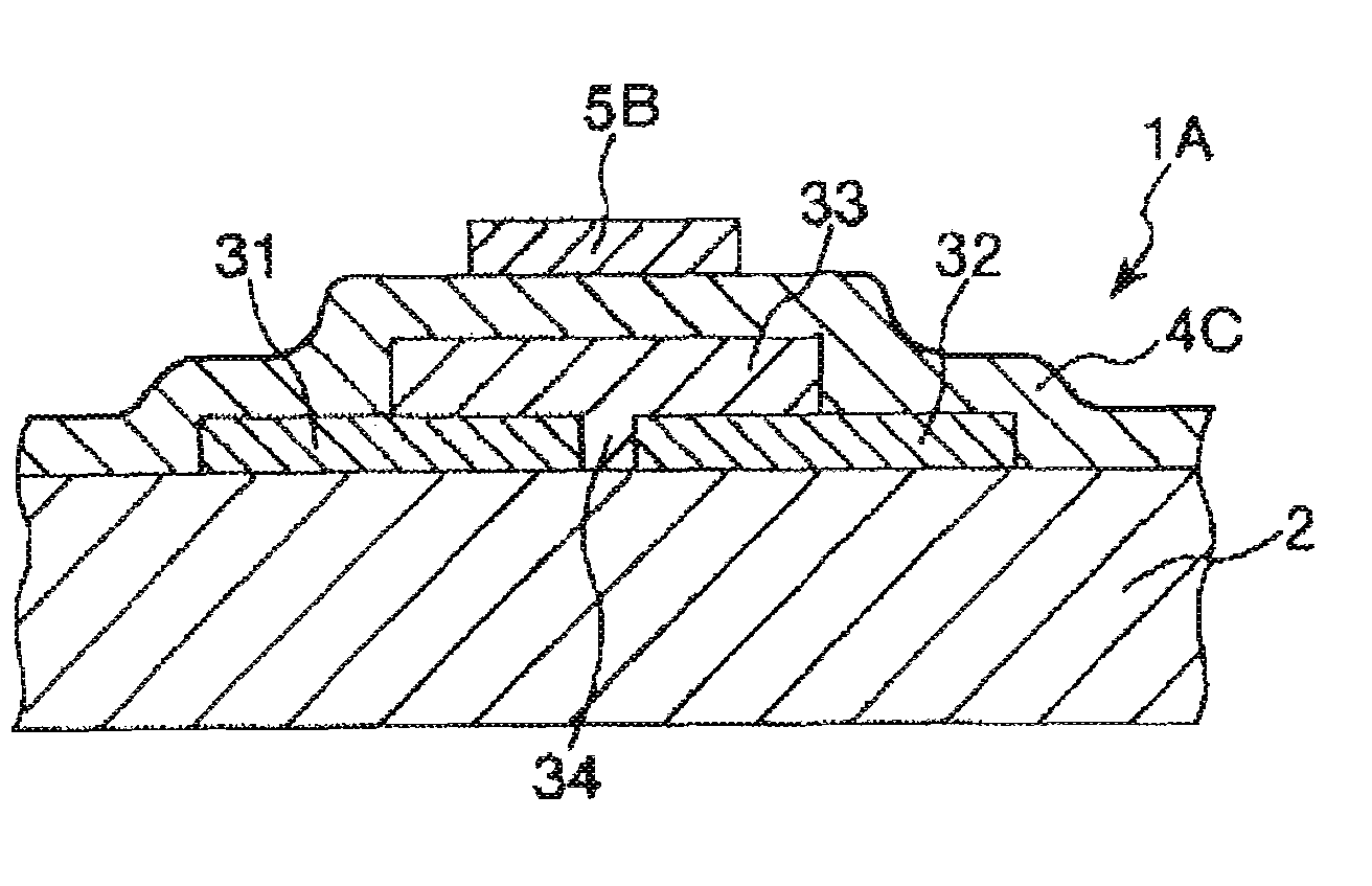
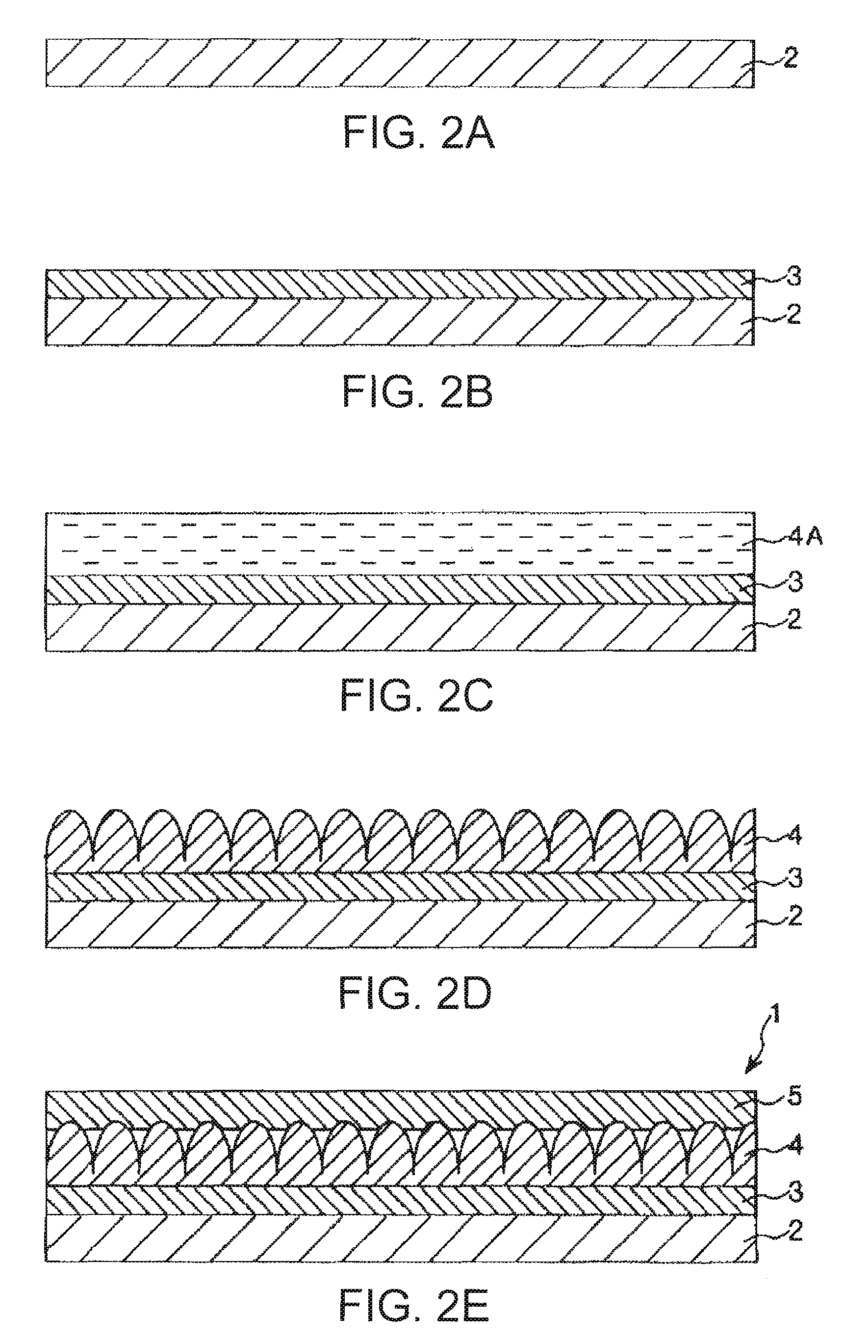
[0049]A memory element in other words a memory element formed by a method for manufacturing a memory element according to the first embodiment is described with reference to FIG. 1.

[0050]FIG. 1 is a longitudinal sectional view of a memory element according to the first embodiment. The upper side in FIG. 1 is hereinafter referred as the “upper side” and the lower side in FIG. 1 is referred as the “lower side” for convenience of explanation. The memory element 1 shown in FIG. 1 includes a substrate 2, on top of which there is a first electrode 3 (a lower electrode), on top of which there is a ferroelectric layer 4 (a recording layer), and on top of which there is a second electrode 5 (an upper electrode). In other words, in the memory element 1, a structure (or a capacitor) including the ferroelectric layer 4 between the first electrode 3 and the second electrode 5 is supported by the substrate 2 in...

Example

[0130]A second embodiment of the invention is now described with reference to FIG. 5.

[0131]FIG. 5 is a schematic sectional view of film forming equipment which is used in a method for manufacturing a memory element according to the second embodiment.

[0132]In the following description, structures or elements of the second embodiment which are different from those of the first embodiment described above will be mainly described and explanations for the same elements and configurations as those of the first embodiment will be omitted.

[0133]The second embodiment is almost same as the first embodiment other than the film forming equipment used to form the ferroelectric layer 4.

[0134]More specifically, film forming equipment 10A according to the second embodiment has a substrate holder 12A that holds the substrate 2. The substrate holder 12A is supported through the rotation shaft 15 that can rotate around the axis extending in the thickness direction of the substrate 2 and by a rotation ...

Example

[0136]A third embodiment of the invention is now described with reference to FIG. 6.

[0137]FIG. 6 is a schematic sectional view of film forming equipment which is used in a method for manufacturing a memory element according to the third embodiment.

[0138]In the following description, structures or elements of the third embodiment which are different from those of the first embodiment described above will be mainly described and explanations for the same elements and configurations as those of the first embodiment will be omitted.

[0139]The third embodiment is almost same as the first embodiment other than a structure of the film forming equipment used to form the ferroelectric layer 4.

[0140]Referring to FIG. 6, a material supplying source 13A containing the electrode material 5A and a substrate holder 12C for holding the substrate 2 are provided in a chamber (unshown) in third embodiment. A slit plate 16 that has a slit-shaped opening 16A is further provided between the material suppl...


PUM


Abstract

A method for manufacturing a memory element including forming a first electrode on a first face of a substrate; forming a ferroelectric layer on a second face of the first electrode, the second face being on an opposite side to the substrate side, and the ferroelectric layer being mainly made of a crystalline organic ferroelectric material; and forming a second electrode on a third face of the ferroelectric layer, the third face being on an opposite side to the first electrode side, the second electrode being formed by ejecting an vaporized electrode material in a direction inclined with respect to a normal line direction of the substrate and depositing the vaporized electrode material on the third face of the ferroelectric layer, wherein data writing/reading is performed by changing a polarized state of the ferroelectric layer by applying a voltage between the first electrode and the second electrode.

Description

BACKGROUND OF THE INVENTION[0001]1. Technical Field[0002]Several aspects of the present invention relate to a memory element, a method for manufacturing a memory element, a memory device, an electronic apparatus and a method for manufacturing a transistor.[0003]2. Related Art[0004]A memory element made of ferroelectric material has been known. In the memory element, an electric field is applied to a ferroelectric layer made of the ferroelectric material in its thickness direction. This elemenet changes its polarized state and in this way writing and reading of data is performed. The polarized state in the ferroelectric layer is bistable and retained even after the application of the electric field has stopped thereby such memory element can be used as a nonvolatile memory.[0005]Use of an organic ferroelectric material has been recently proposed as the ferroelectric material forming such memory element in order to make the memory element flexible. Journal of Applied Physics, Vol. 89,...

Claims


Application Information

Patent Timeline
IPC IPC(8): H01L21/00H01L21/8238H01L21/8242
CPCH01L21/28291H01L21/6715H01L21/68764H01L29/78391H01L27/1159H01L28/55H01L29/516H01L27/11585H01L29/40111H10B51/00H10B51/30
Inventor TAKIGUCHI, HIROSHIKARASAWA, JUNICHI
Owner SEIKO EPSON CORP
Why Eureka
Try Eureka