

Light Emitting Element
- Summary
- Abstract
- Description
- Claims
- Application Information
AI Technical Summary
Benefits of technology
Problems solved by technology
Method used
Image

Examples
embodiment mode 1
[0064] One mode of the composite material of the invention is a structure including an organic compound and an inorganic compound which shows an electron-accepting property to the organic compound. At this time, the composite material is made to have a property of an impurity semiconductor (p-type) having a high impurity concentration by mixing a large amount of inorganic compounds showing an electron-accepting property. In other words, a conduction mechanism is band conduction.
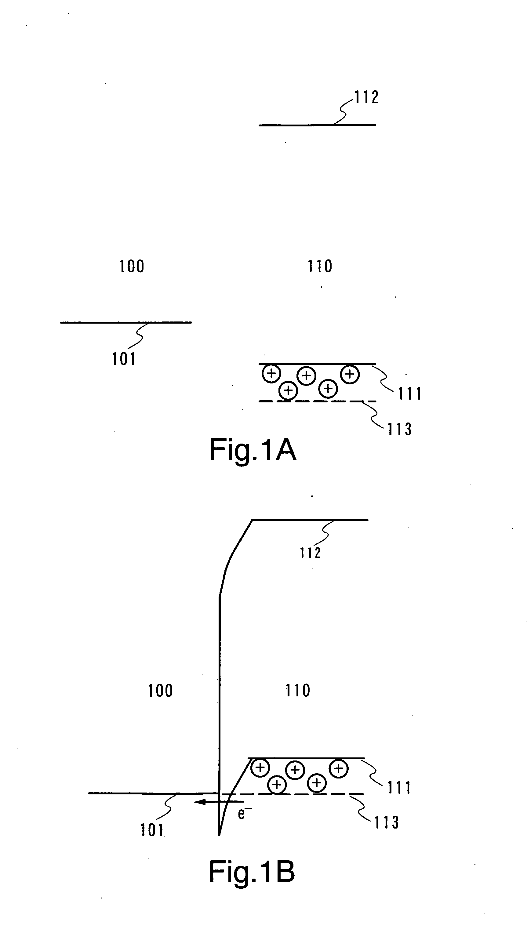
[0065] In the case of having a property of the impurity semiconductor (p-type) having a high impurity concentration, a schematic diagram of an energy level when a hole is injected from an electrode 100 into a composite material 110 of the invention is as shown in FIGS. 1A and 1B. FIG. 1A schematically shows a state before the electrode 100 has contact with the composite material 110 of the invention. Reference numeral 101 denotes a Fermi level of the electrode 100; 111, an upper limit of a valence band of th...
embodiment mode 2
[0083] Embodiment Mode 2 explains a current-excitation light emitting element using such a composite material of the present invention as described in Embodiment Mode 1. A typical element structure is shown in FIG. 3. The light emitting element of the invention includes a first layer 311 formed from such a composite material of the invention as described in Embodiment Mode 1 and a second layer 312 containing a light emitting material between a first electrode 301 and a second electrode 302, in which the first layer 311 is provided in contact with the first electrode 301.
[0084] Embodiment Mode 2 exemplifies an element in which current flows when a potential of the first electrode 301 is higher than that of the second electrode 302, and a hole 321 and an electron 322 are recombined with each other in the second layer 312 to emit light. Thus, the first electrode 301 serves as an anode.
[0085] As described in Embodiment Mode 1, when a work function of a material for forming the first e...
embodiment mode 3
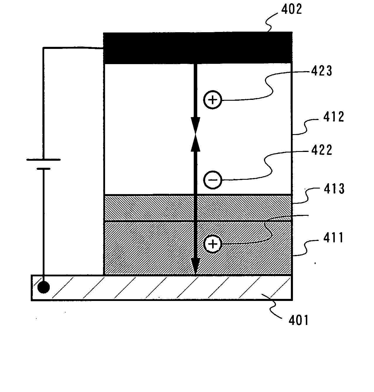
[0094] Embodiment Mode 3 explains one mode of the light emitting element of the present invention, which is different from that in Embodiment Mode 1. An element structure is shown in FIG. 4. A light emitting element of Embodiment Mode 3 includes a first layer 411 formed from the composite material of the invention as described in Embodiment Mode 1 and a second layer 412 containing a light emitting material between a first electrode 401 and a second electrode 402, in which the first layer 411 is provided in contact with the first electrode 401. In addition, a third layer 413 which generates electrons is provided between the first layer 411 and the second layer 412.
[0095] In Embodiment Mode 3, current flows when a potential of the first electrode 401 is lower than that of the second electrode 402. At this time, an electron 422 injected from the third layer 413 into the second layer 412 and a hole 423 injected from the second electrode 402 are recombined with each other in the second ...
PUM
| Property | Measurement | Unit |
|---|---|---|
| Thickness | aaaaa | aaaaa |
| Thickness | aaaaa | aaaaa |
| Energy | aaaaa | aaaaa |
Abstract
Description
Claims
Application Information