Compound for organic electric element, organic electric element using same, and electronic apparatus thereof
Active Publication Date: 2018-08-09
DUK SAN NEOLUX
View PDF2 Cites 7 Cited by
Summary
Abstract
Description
Claims
Application Information
AI Technical Summary
This helps you quickly interpret patents by identifying the three key elements:
Problems solved by technology
Method used
Benefits of technology
Benefits of technology
The present invention provides a compound that can improve the efficiency and lifespan of organic electric devices by using deuterium to block electron movement and transport holes. This results in lower driving voltages, increased luminous efficiency, and better heat resistance. Additionally, an organic electric element comprising this compound has better color purity and lifetime.
Problems solved by technology
Currently, the major overcoming problem of organic light emitting devices is that the problem of power consumption and lifetime must be solved as the panel size of a mobile phone or a tablet PC becomes larger.
However, it is difficult to simultaneously overcome the driving voltage and the lifetime solely by the hole transporting layer material.
In the case of a molecule in which planar structures are excessively introduced, holes are trapped and stabilized between the plate structures when the constant current is continuously supplied in the evaluation of device lifetime, so that the hole mobility is lowered, as a result, the driving voltage rises in order to apply a constant current, resulting in an adverse effect on the lifetime of the device.
This may bring about a very fatal effect on the lifetime.
Therefore, as described above, introduction of a certain number or more of the plate structure capable of increasing the hole mobility cause a harmful effect on the lifetime, and thus, there is a limit to lowering the driving voltage by using it.
However, many studies have not been conducted on a hole transporting material which can lower the driving voltage and improve the hole transfer ability by substituting with deuterium, and accordingly, it is strongly required to develop materials of the emission-auxiliary layer and the hole transport layer.
Method used
Image
Click on the blue label to locate the original text in one second.
Reading with bidirectional positioning of images and text.
Examples
synthesis example
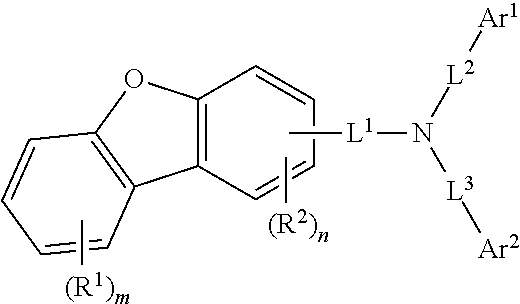
[0087]The compound (final products) represented by Formula 1 according to the present invention are synthesized by reacting Sub 1 and Sub 2 as shown in Reaction Scheme 1, but are not limited thereto.
[0088]I. Synthesis of Sub 1
[0089]Sub 1 of the Reaction Scheme 1 can be synthesized according to, but not limited to, the reaction route of the following Reaction Scheme 2.
[0090]Here, Hal1 may be Br or I.
[0091]Synthesis Examples of compounds comprised in Sub 1 are as follows.
1. Synthesis Example of Sub 1-3
[0092]
[0093](1) Synthesis of Sub 1-I-3
[0094]The starting material 3-bromo-[1,1′-biphenyl]-2-ol (59.89 g, 240.43 mmol) was placed in a round bottom flask together with Pd(OAc)2 (5.40 g, 24.04 mmol), 3-nitropyridine (2.98 g, 24.04 mmol), and dissolved in C6F6 (360 ml) and DMI (240 ml). Then, tert-butyl peroxybenzoate (93.40 g, 480.85 mmol) was added and the stirring at 90° C. was followed. When the reaction was completed, the reaction product was extracted with CH2Cl2 and water, and then, ...
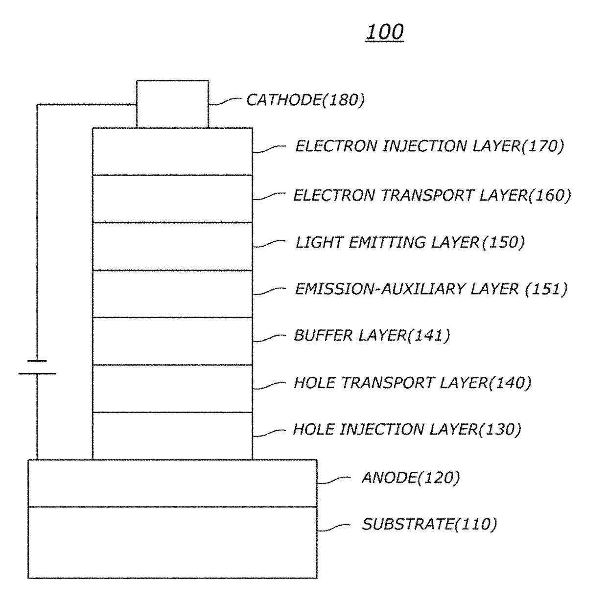
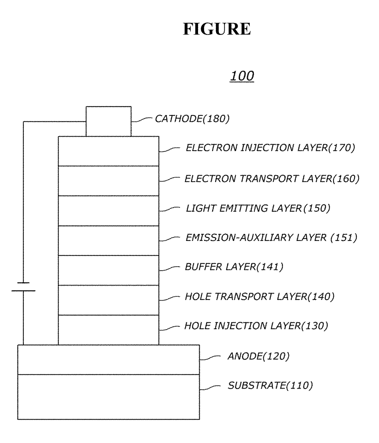
[0178]Organic light emitting diodes (OLEDs) were fabricated according to a conventional method by using a compound of the present invention as a hole transport layer material.
[0179]First, an ITO layer (anode) was formed on a glass substrate, and then 4,4′,4″-tris[2-naphthyl(phenyl)amino]triphenylamine (hereinafter, “2-TNATA”) was vacuum-deposited on the ITO layer to form a hole injection layer with a thickness of 60 nm. Subsequently, compound P-1 of the present invention was vacuum-deposited with a thickness of 60 nm on the hole injection layer to form a hole transport layer. Subsequently, a light emitting layer with a thickness of 30 nm was formed on the hole transport layer by using 4,4′-N,N′-dicarbazole-biphenyl (hereinafter, “CBP”) as a host material and tris(2-phenylpyridine)-iridium (hereinafter, “Ir(ppy)3)”) as a dopant material in a weight ratio of 90:10.
[0181]The OLEDs were fabricated in the same manner as described in Example I-1 except that the compounds P-2 to P-60 of the present invention described in Table 4 instead of the compound P-1 of the present invention were used as the hole transport layer material.
PUM
Property
Measurement
Unit
Fraction
aaaaa
aaaaa
Length
aaaaa
aaaaa
Length
aaaaa
aaaaa
Abstract
Provided are a compound capable of lowering a driving voltage, enhancing light emitting efficiency and thermal resistance, and improving lifespan and color purity of the element, an organic element using the same, and an electric device for the same.
Description
CROSS-REFERENCE TO RELATED APPLICATION[0001]This application claims priority from and the benefit under 35 U.S.C. § 119(a) of Korean Patent Application No. 10-2015-0090751 filed on Jun. 25, 2015, the contents of which are hereby incorporated by reference for all purposes as if fully set forth herein.BACKGROUNDTechnical Field[0002]The present invention relates to compounds for organic electric elements, organic electric elements using the same, and electronic devices thereof.Background Art[0003]Flat panel display devices are playing a very important role in supporting a high image information society, showing rapid growth mainly in the Internet in recent years.[0004]In particular, an organic electroluminescent device (organic EL device) capable of being driven at low voltage as self-luminous type has excellent viewing angle and contrast ratio, is lightweight and thin because no backlight is required, and has advantages in terms of power consumption, compared with liquid crystal displ...
Claims
Application Information
Patent Timeline
Application Date:The date an application was filed.
Publication Date:The date a patent or application was officially published.
First Publication Date:The earliest publication date of a patent with the same application number.
Issue Date:Publication date of the patent grant document.
PCT Entry Date:The Entry date of PCT National Phase.
Estimated Expiry Date:The statutory expiry date of a patent right according to the Patent Law, and it is the longest term of protection that the patent right can achieve without the termination of the patent right due to other reasons(Term extension factor has been taken into account ).
Invalid Date:Actual expiry date is based on effective date or publication date of legal transaction data of invalid patent.

