Microwave Plasma Processing Apparatus

a plasma processing and microwave technology, applied in the direction of vacuum evaporation coating, plasma technique, coating, etc., can solve the problems of difficult to uniformly plasma-process a large-size semiconductor wafer at an increased speed, fine-size element damage, etc., to ensure the uniformity and stability of plasma, increase the uniformity and stability, and ensure the effect of uniformity and stability

Inactive Publication Date: 2007-12-13
TOKYO ELECTRON LTD
View PDF4 Cites 12 Cited by
  • Summary
  • Abstract
  • Description
  • Claims
  • Application Information

AI Technical Summary

Benefits of technology

[0039] In accordance with the present invention, two or more holes extend from an end portion of a microwave transmitting board into the plate so that microwaves arriving at the microwave transmitting board via a planar antenna can be propagated into the holes. Furthermore, a volume adjustment mechanism is provided to adjust volumes of the holes. When the microwave transmitting board is divided into individual units to which each of the two or more holes belongs, impedance of the individual units is controlled to thereby control an electric field distribution of the microwave transmitting board by adjusting the volumes of the holes with the volume adjustment mechanism. Thus, in the event that process conditions or the like are changed it is possible to assure increased uniformity and stability of plasma by controlling the electric field distribution of the microwave transmitting board through a simple operation but without having to optimize a pattern of microwave radiation holes of a planar antenna and a microwave transmitting board.
[0040] More specifically, when the microwave transmitting board is divided into individual units to which each of the two or more holes belongs, the electric field distribution of the microwave transmitting board can be made uniform by controlling the impedance of the individual units and allowing each of the units to satisfy resonance conditions. This helps to realize a plasma processing with increased uniformity and stability.

Problems solved by technology

In cases of a parallel plate plasma processing apparatus and an inductively-coupled plasma processing apparatus, both of which have been extensively used in the art, plasma damage may occur in a fine-size element due to an increased temperature of electrons.
Further, since a plasma density is kept high only in a limited region, it is difficult to uniformly plasma-process a large-size semiconductor wafer at an increased speed.

Method used


Image

  • Microwave Plasma Processing Apparatus
  • Microwave Plasma Processing Apparatus
  • Microwave Plasma Processing Apparatus

Examples


Embodiment Construction

[0051] Hereinafter, embodiments of the present invention will be described in detail with reference to the accompanying drawings.

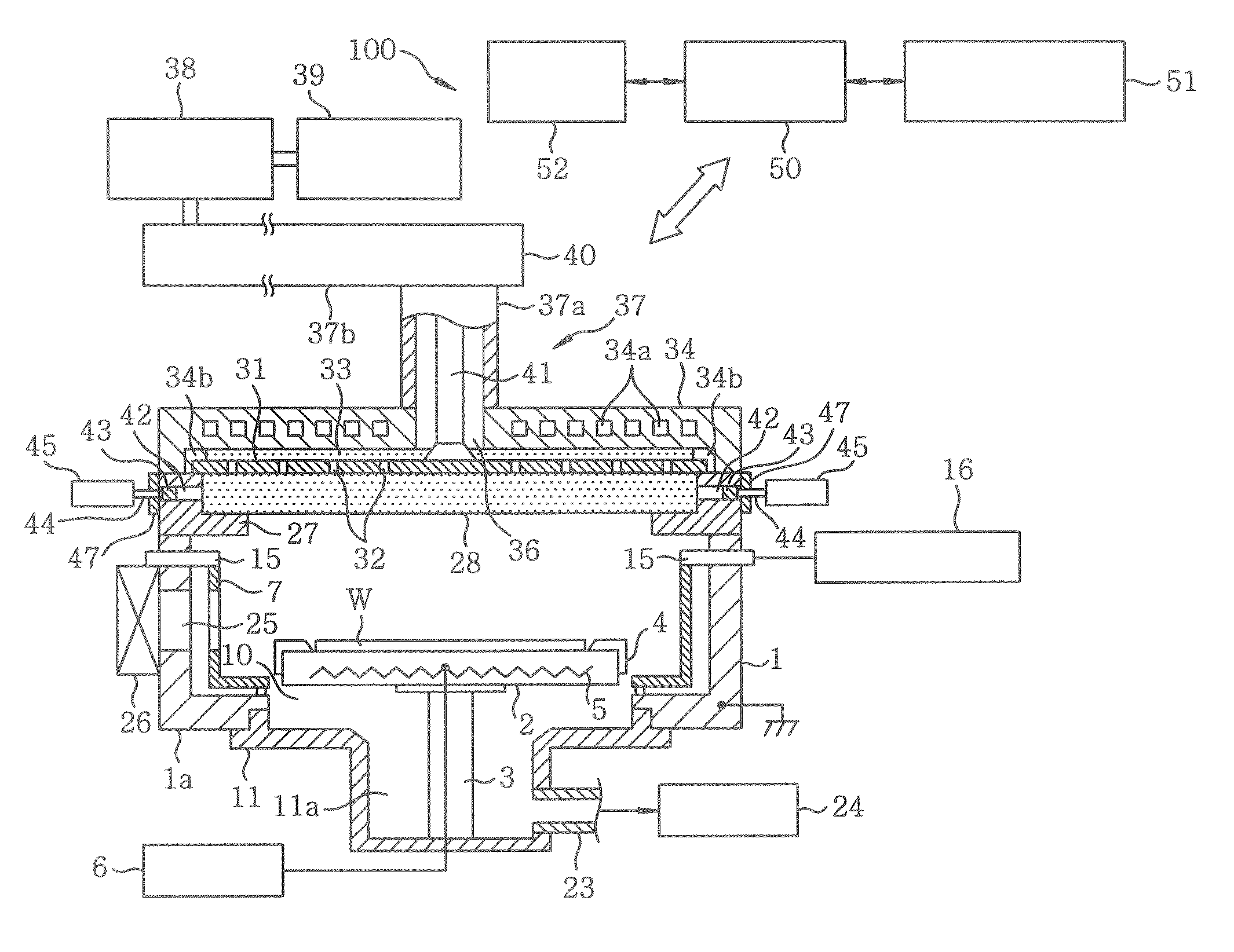
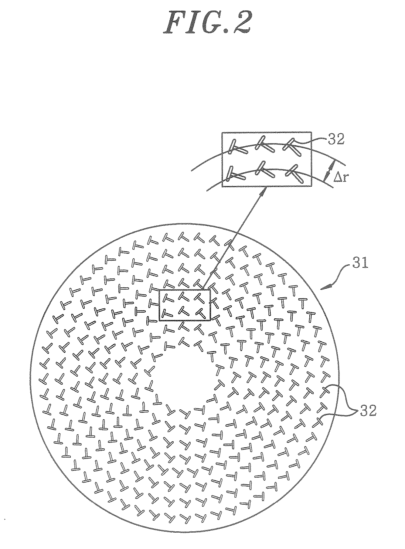
[0052]FIG. 1 is a section view showing a frame format of a microwave plasma processing apparatus in accordance with one embodiment of the present invention.

[0053] The microwave plasma processing apparatus 100 is configured with a RLSA type microwave plasma processing apparatus that produces plasma by irradiating microwaves generated from a microwave generator into a chamber by use of a planar antenna (a radial line slot antenna) having a multiple number of slots formed in a specified pattern.

[0054] The microwave plasma processing apparatus 100 includes a substantially cylindrical chamber 1 airtiqhtly sealed and grounded. A circular opening 10 is provided at an approximately central portion of a bottom wall 1a of the chamber 1. An exhaust chamber 11 communicates with the opening 10 and protrudes downwardly from the bottom wall 1a. Within the chamber 1, t...


PUM

PropertyMeasurementUnit
frequencyaaaaaaaaaa
frequencyaaaaaaaaaa
frequencyaaaaaaaaaa

Abstract

A microwave plasma processing apparatus which easily ensures uniformity and stability of plasma in response to changes of process conditions and the like. The microwave plasma processing apparatus 100 generates plasma of a process gas in a chamber by microwave and performs plasma processing to a work to be processed by using the plasma. On a plate 27 composed of a conductor covering the outer circumference of a micro wave transmitting board 28, two or more holes 42 for propagating microwave from an edge part of the microwave transmitting board 28 to an inner part of the holes 42 are formed. Volume adjusting mechanisms 43 and 45 adjust the volume of the holes to adjust impedance of each unit when the microwave transmitting board 28 is divided by unit to which each of the holes 42 belongs, and electric field distribution of the microwave transmitting board 28 is controlled.

Description

FIELD OF THE INVENTION [0001] The present invention relates to a microwave plasma processing apparatus by which an object is processed by microwave plasma. BACKGROUND OF THE INVENTION [0002] A plasma processing is a technique indispensable to the manufacture of semiconductor devices. In recent years, a design rule for semiconductor elements constituting an LSI becomes gradually miniaturized with a view to comply with a demand for high-integration and high-speed LSI, and a semiconductor wafer grows in size. In keeping with this trend, a plasma processing apparatus is required to cope with the miniaturization and the size growth. [0003] In cases of a parallel plate plasma processing apparatus and an inductively-coupled plasma processing apparatus, both of which have been extensively used in the art, plasma damage may occur in a fine-size element due to an increased temperature of electrons. Further, since a plasma density is kept high only in a limited region, it is difficult to unifo...

Claims


Application Information

Patent Timeline
Patent Type & Authority Applications(United States)
IPC IPC(8): H01L21/3065C23C16/00
CPCC23C16/511H01J37/32192H01J37/32266H01J37/32238H01J37/3222H01L21/3065H05H1/46
Inventor TIAN, CAIZHONGNOZAWA, TOSHIHISA
Owner TOKYO ELECTRON LTD
Why Eureka
Try Eureka