High-speed CMOS current mirror

a cmos current mirror, high-speed technology, applied in the direction of amplifiers with semiconductor devices only, instruments, etc., can solve problems such as troublesome delays in some applications

Active Publication Date: 2007-12-13
ATMEL CORP
View PDF10 Cites 16 Cited by
  • Summary
  • Abstract
  • Description
  • Claims
  • Application Information

AI Technical Summary

Benefits of technology

[0027] As a desired result, this embodiment permits a contin...

Problems solved by technology

This delay is trouble...

Method used


Image

  • High-speed CMOS current mirror
  • High-speed CMOS current mirror
  • High-speed CMOS current mirror

Examples


Embodiment Construction

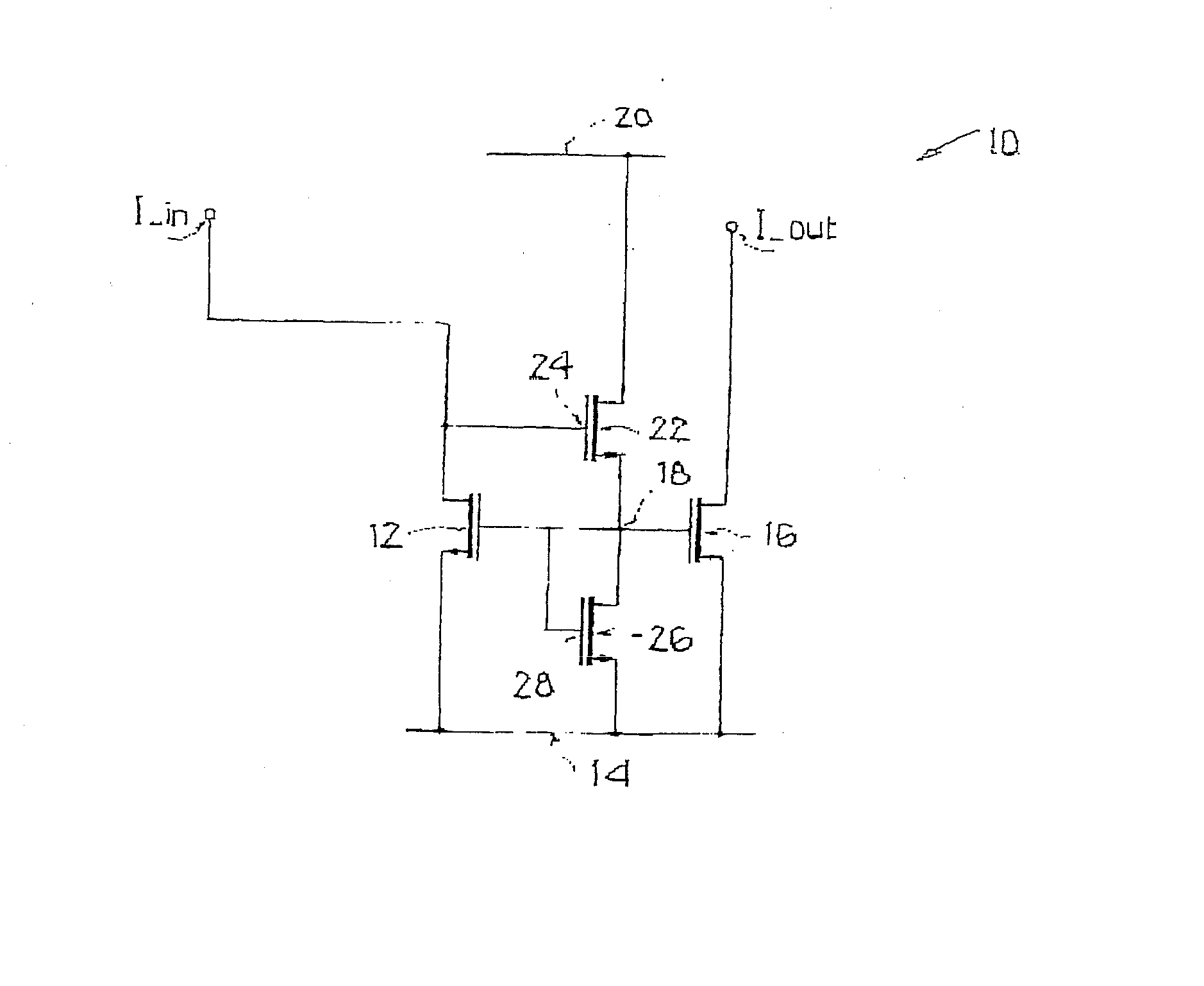
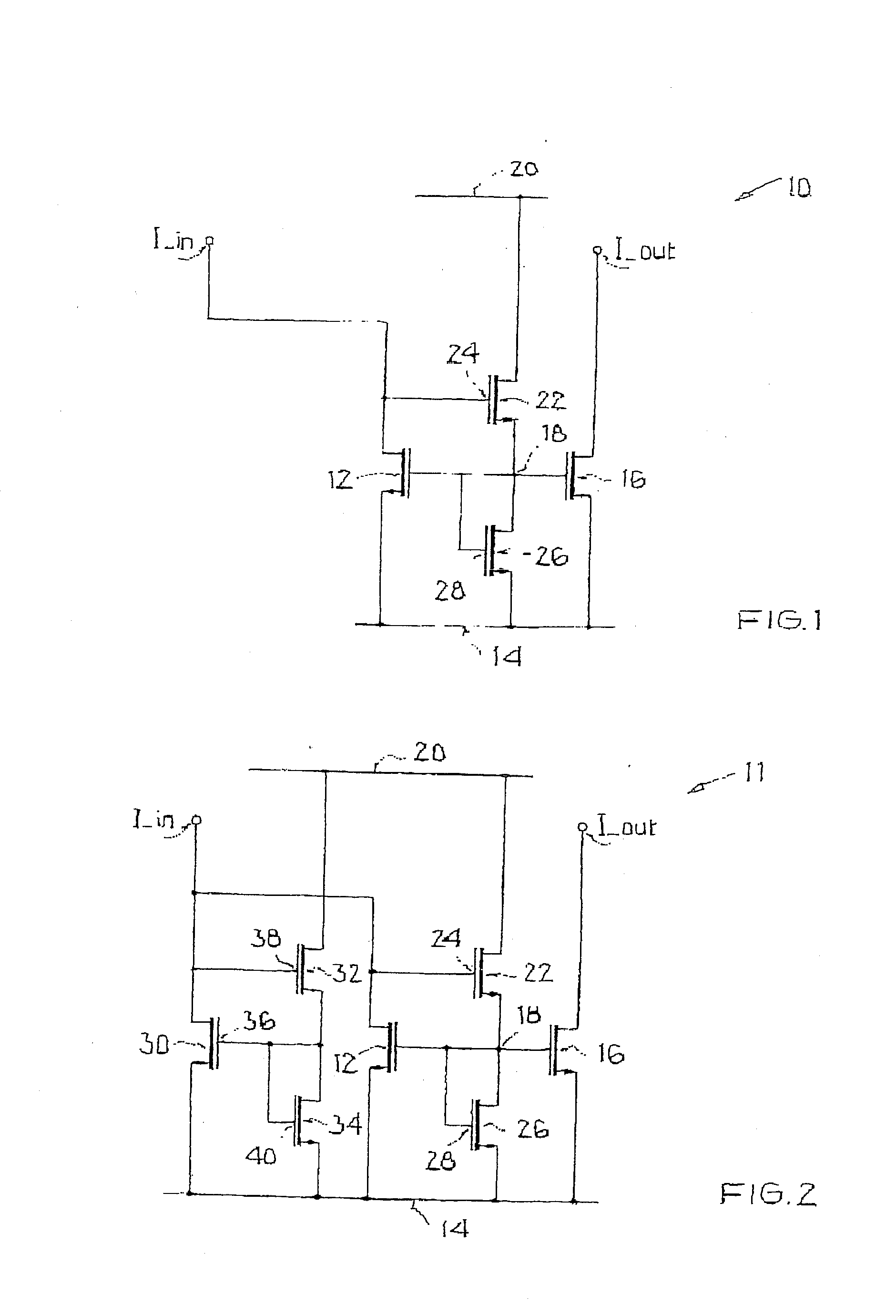
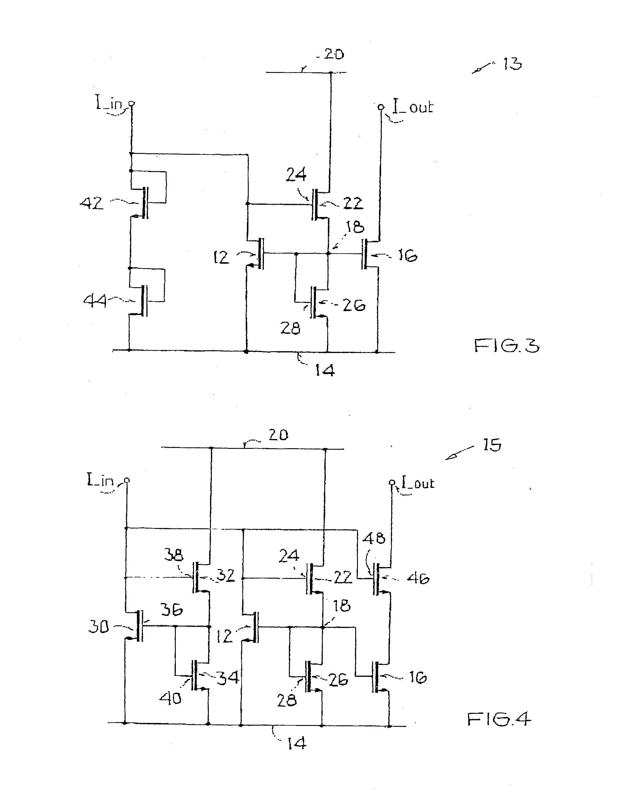
[0039]FIG. 1 shows a CMOS current mirror 10 with a current input I_in, an input transistor 12, a reference potential terminal 14, a current output I_out, and an output transistor 16. The conductivity path of input transistor 12 is located between the first current input I_in and reference potential terminal 14. The conductivity path of output transistor 16 is located between the current output I_out and reference potential terminal 14. Gate terminals of both transistors 12, 16 are connected to a common gate node 18. Current mirror 10 furthermore has a supply potential terminal 20. A first additional transistor 22 has a conductivity path, located between supply potential terminal 20 and gate node 18. Gate terminal 24 of first additional transistor 22 is connected to the current input I_in. The conductivity path of a second additional transistor 26 is located between gate node 18 and reference potential terminal 14. Gate terminal 28 of second additional transistor 26 is also connected...


PUM


Abstract

A CMOS current mirror is provided that includes a current input, an input transistor, whose conductivity path is located between the current input and a reference potential terminal, a current output, an output transistor, whose conductivity path is connected to the reference potential terminal and which supplies the current output with an output current, a gate node common for both transistors, and a supply potential terminal. The current mirror further includes a first additional transistor, whose conductivity path is located between the supply potential terminal and the gate node and whose gate terminal is connected to the current input, and a second additional transistor, whose conductivity path is located between the gate node and the reference potential terminal and whose gate terminal is connected to the gate node.

Description

[0001] This nonprovisional application claims priority under 35 U.S.C. § 119(a) on German Patent Application No. 102006017989, which was filed in Germany on Apr. 7, 2006, and which is herein incorporated by reference. BACKGROUND OF THE INVENTION [0002] 1. Field of the Invention [0003] The present invention relates to a CMOS current mirror. [0004] 2. Description of the Background Art [0005] A type of CMOS current mirror is known, for example, from Tietze / Schenk, “Halbleiterschaltungstechnik” (Semiconductor Technology), ISBN 3-540-19475-4, 9th ed., Springer-Verlag, Berlin / Heidelberg / New York, pp. 96 and 97. A current mirror with a resistor between gate terminals of an input and output transistor is known furthermore from the publication “A Novel Highspeed Current Mirror Compensation Technique and Application”, Thart Fah Voo, Toumazou, C., IEEE International Symposium on Circuits and Systems; 1995, Vol. 3, 28 Apr. to 3 May 1995, pages: 2108 to 2111. Furthermore, current mirrors with ca...

Claims


Application Information

Patent Timeline
IPC IPC(8): H03F3/04
CPCG05F3/262
Inventor KARTHAUS, UDOKOLB, PETER
Owner ATMEL CORP
Why Eureka
Try Eureka