System and method for exposing electronic substrates to UV light

a technology of ultraviolet light and electronic substrates, applied in the field of flash lamp exposure systems, can solve the problems of comparatively low power, fragile current system, and complicated shutter mechanism

Inactive Publication Date: 2007-12-13
ORC IMAGING CORP
View PDF10 Cites 42 Cited by
  • Summary
  • Abstract
  • Description
  • Claims
  • Application Information

AI Technical Summary

Benefits of technology

[0008]These and other aspects of the invention will be more readily comp

Problems solved by technology

Furthermore, current systems are fragile, employ complicated shutter mechanisms to apply dosages and are comparatively low in power.
The long exposure times and poor heat filtering of current systems add heat to the substrate,

Method used


Image

  • System and method for exposing electronic substrates to UV light
  • System and method for exposing electronic substrates to UV light
  • System and method for exposing electronic substrates to UV light

Examples


Embodiment Construction

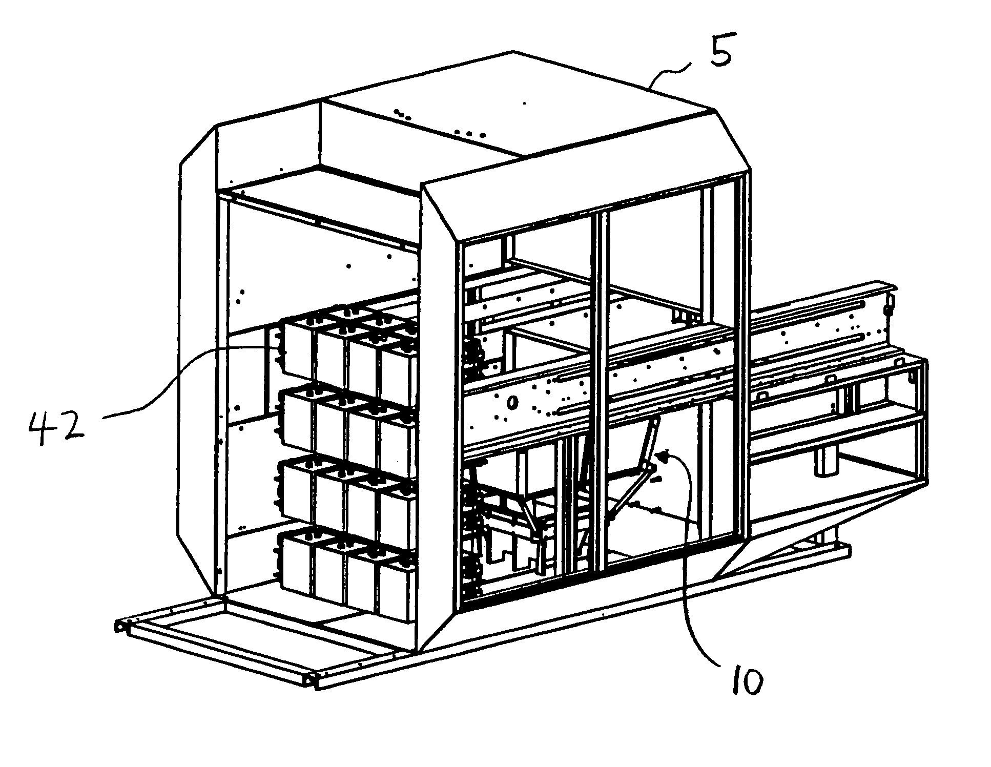
[0031]The present invention relates to a rapid exposure of photopolymer resists (i.e., photoresists) to ultraviolet (UV) radiation (i.e., UV light). More particularly, the present invention relates to a system and method for exposing an electronic substrate to UV light to cure the photoresists at a faster speed (e.g., takes 2 seconds) than the speed (e.g., takes 30 to 40 seconds) of the conventional systems. Although the present invention will be described hereinafter primarily in the context of exposing photopolymers to UV light during the production of electronic circuit boards, one skilled in the art would appreciate that the present invention is not limited thereto, and can be used in various other applications. Further, while the present invention is primarily applicable to solder mask applications to speed up the process, it is also suitable to other applications such as applications involving liquid resists or dry film.

[0032]In one exemplary embodiment in accordance with the ...


PUM


Abstract

A flash lamp exposure system for exposing a substrate to ultraviolet radiation. The system includes at least one flash lamp, each of which includes: at least one lamp for emitting ultraviolet radiation in response to a voltage; at least one first reflector, each first reflector being adapted to reflect the ultraviolet radiation toward the substrate; a second reflector surrounding a path of the ultraviolet radiation from the at least one lamp to the substrate, the second reflector being adapted to reflect first rays of the ultraviolet radiation toward the substrate; and a third reflector disposed closer to the substrate than the secondary reflector and surrounding the path of the ultraviolet radiation from the at least one lamp to the substrate, the third reflector being adapted to reflect second rays of the ultraviolet radiation toward the substrate.

Description

FIELD OF THE INVENTION[0001]The present invention relates to a system and method for rapidly exposing electronic substrates to ultraviolet light, and more particularly to a flash lamp exposure system that reduces photoresist curing time.BACKGROUND OF INVENTION[0002]The exposure of photopolymer resists (i.e., photoresists) used in the fabrication of electronic substrates (e.g., for solder masks) requires tremendous amounts of energy at wavelengths at ultraviolet (UV) region of the spectrum (e.g., in the range of 350 nm to 450 nm). Light sources currently used for such UV light exposure include mercury xenon short arc lamps and metal halide extended arc lamps, that can require 30 to 40 seconds or more to expose such resists. This long exposure time is generally needed to deliver the approximately 200 to 800 milli-Joules (mJ) or more (e.g., more than 1000 mJ / cm2) of energy necessary to fully and properly expose high energy resists.[0003]Furthermore, current systems are fragile, employ ...

Claims


Application Information

Patent Timeline
IPC IPC(8): G03C1/52
CPCG03F7/2032G03F7/2008
Inventor JACOBO, VICTOR M.SINGH, RAJA D.SOUKASIAN, ANDREJACOBSEN, DAVID A.FABELA, FRANK E.
Owner ORC IMAGING CORP
Why Eureka
Try Eureka