
Eureka
For R&D, Eureka makes reading and utilizing patents & technical documents easy.
Eureka AIR
Designed for self-driven R&D workflows. Generate viable solutions, solve complex R&D challenges, empower your innovation with AI.

Eureka Materials
Designed for material experts only. Revolutionize your material R&D, from search, analyze, to developing new materials.

TechResearch
Generate reliable direction feasibility study reports for your R&D in just a few steps.

TechSeek
Discover and master advanced knowledge NOW. Basics, ideas, possibilities, all at once.

TechMind
As an expert in R&D Theories, TechMind can generates customized viable solutions instantly.

TechRisk
Analyze your overall solution with one click, know your potential R&D risks in advance.

TechMonitor
Get weekly tech updates, stay abreast of the latest tech innovations and key insights.
Semiconductor memory, and testing method thereof
- Summary
- Abstract
- Description
- Claims
- Application Information
AI Technical Summary
Benefits of technology
Problems solved by technology
Method used
Image

Examples
Embodiment Construction
[0046]Hereinafter, specific description will be given of a preferred embodiment of the present invention with reference to the drawings.
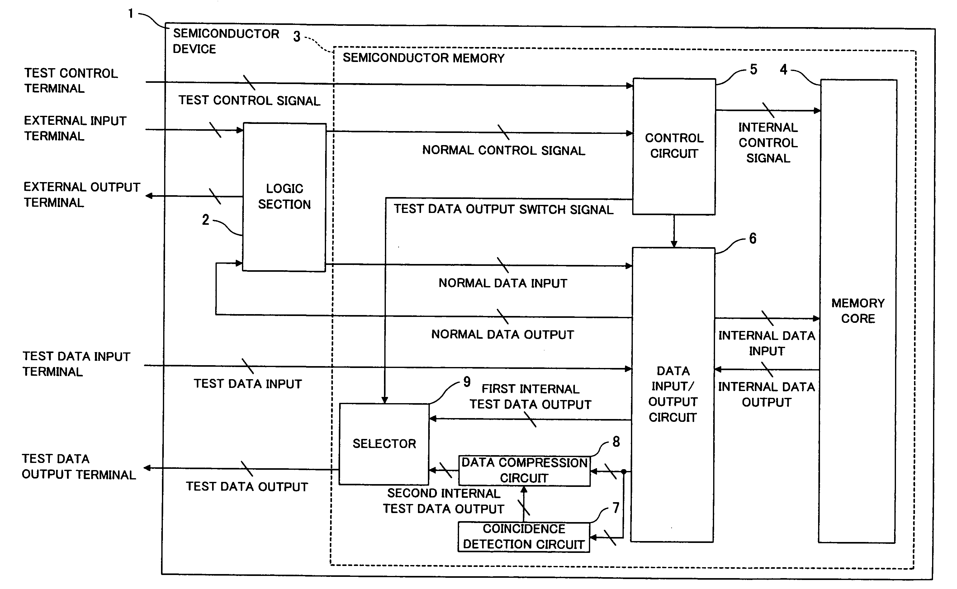
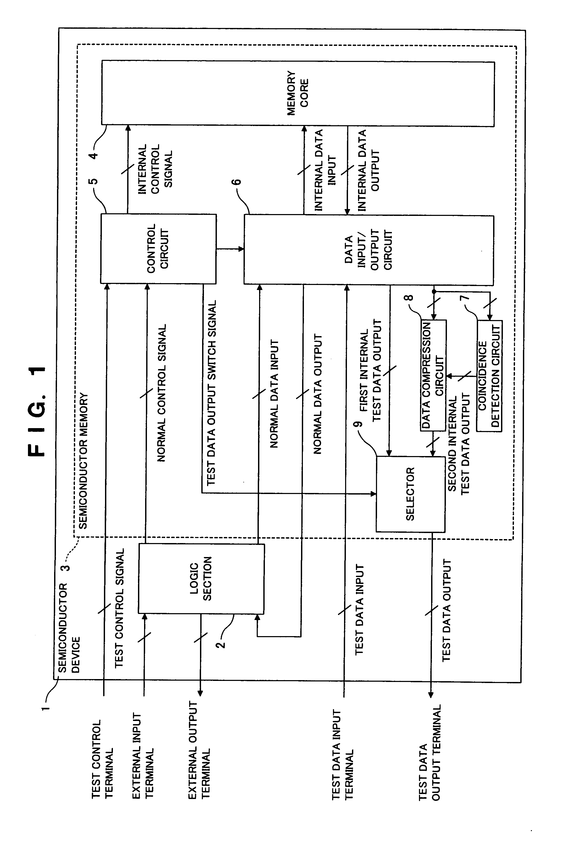
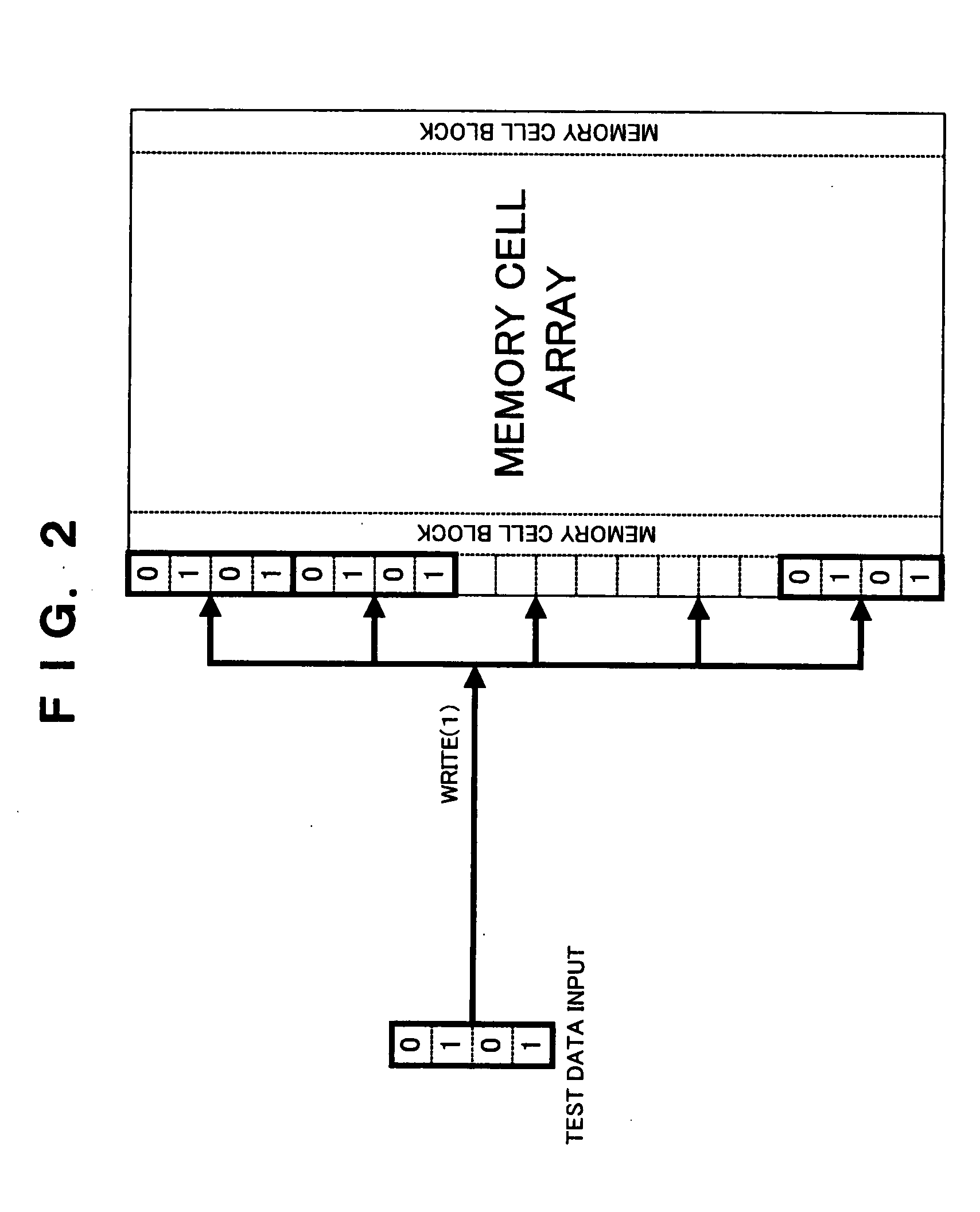
[0047]FIG. 1 illustrates a configuration of a semiconductor device including a semiconductor memory according to the embodiment. FIG. 2 schematically illustrates data write sequences in a test. FIG. 3 schematically illustrates data read sequences in the test. FIG. 4 is a circuit diagram illustrating a read / write enable control circuit forming part of a control circuit 5 illustrated in FIG. 1. FIG. 5 is a circuit diagram illustrating a data input / output circuit 6 illustrated in FIG. 1. FIG. 6 is a circuit diagram illustrating a coincidence detection circuit 7 illustrated in FIG. 1. FIG. 7 is a circuit diagram illustrating a data compression circuit 8 illustrated in FIG. 1.
[0048]As illustrated in FIG. 1, the semiconductor device 1 has a configuration that the semiconductor memory 3 according to the present invention is mounted together with a logic se...
PUM
 Abstract
Description
Claims
Application Information
 - R&D Engineer
- R&D Manager
- IP Professional
- Industry Leading Data Capabilities
- Powerful AI technology
- Patent DNA Extraction
Browse by: Latest US Patents, China's latest patents, Technical Efficacy Thesaurus, Application Domain, Technology Topic, Popular Technical Reports.
© 2024 PatSnap. All rights reserved.Legal|Privacy policy|Modern Slavery Act Transparency Statement|Sitemap|About US| Contact US: help@patsnap.com