Organic light emitting diode display

Inactive Publication Date: 2009-06-11
SAMSUNG DISPLAY CO LTD
View PDF4 Cites 22 Cited by
  • Summary
  • Abstract
  • Description
  • Claims
  • Application Information

AI Technical Summary

Benefits of technology

[0040]In some embodiments, the lifetime of the display device may be increased, and the areas of al

Problems solved by technology

However, the LCD is a passive display device, so it may need an additional light source such as backlight.
Also, the LCD has various problems such as a slow response time and a narrow viewing angle.
Because the OLED display is self-emissive, an additional light source is not necessary, resulting in low power consumption.
However, the lifetime of the OLED display is not optimal if the OLED co

Method used


Image

  • Organic light emitting diode display
  • Organic light emitting diode display
  • Organic light emitting diode display

Examples


Example

Exemplary Embodiment 1

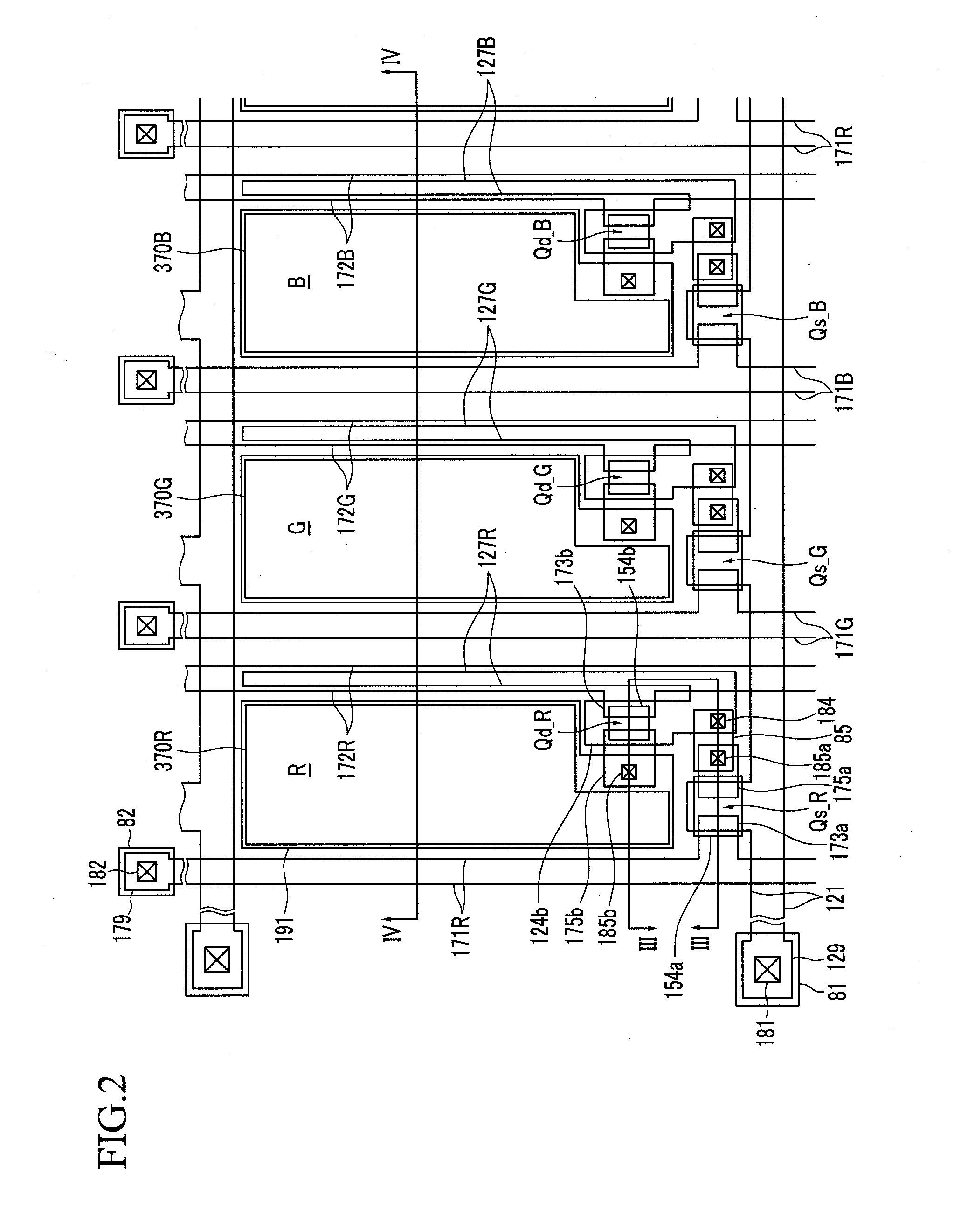
[0052]An OLED display according to an exemplary embodiment of the present invention will now be described in detail with the reference to FIGS. 1 to 4. FIG. 1 is a schematic diagram showing an arrangement of pixels in the OLED display, FIG. 2 is a layout view showing three neighboring pixels in the OLED display of FIG. 1, and FIG. 3 and FIG. 4 show vertical cross-sections marked respectively as III-III and IV-IV in FIG. 2.

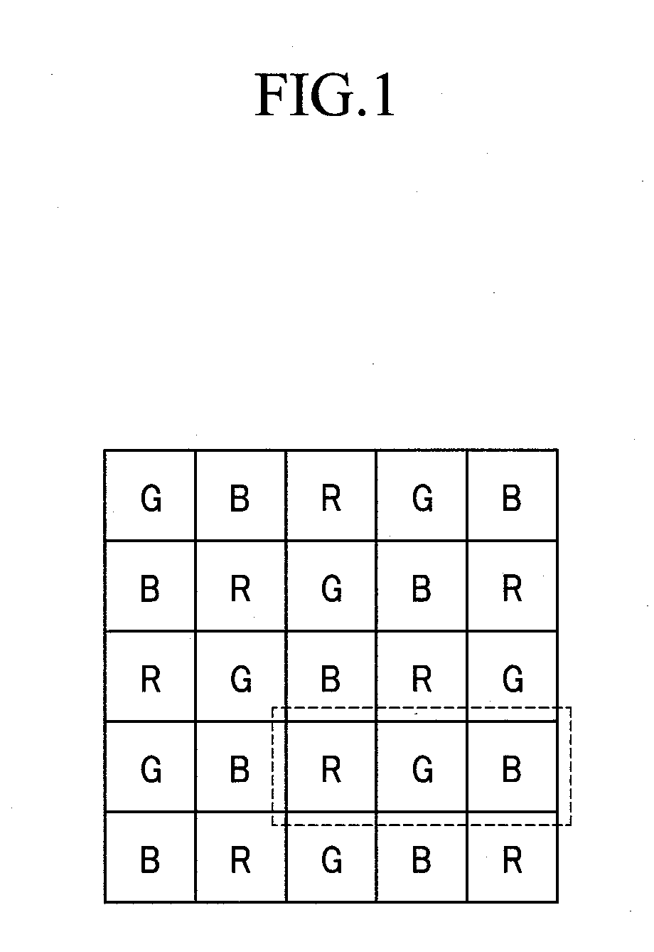
[0053]Referring to FIG. 1, red pixels R, green pixels G, and blue pixels B alternate in the OLED display for displaying respectively red, green, and blue colors. The red, green and blue colors are primary colors used to construct other colors for the display, and pixels of other colors may be used in addition or instead the red, green and blue pixels.

[0054]The pixels are arranged as tripples of a red pixel R, a green pixel G, and a blue pixel B, and these tripples may repeat in each row and column. However, other arrangements and pixel shapes ...

Example

Exemplary Embodiment 2

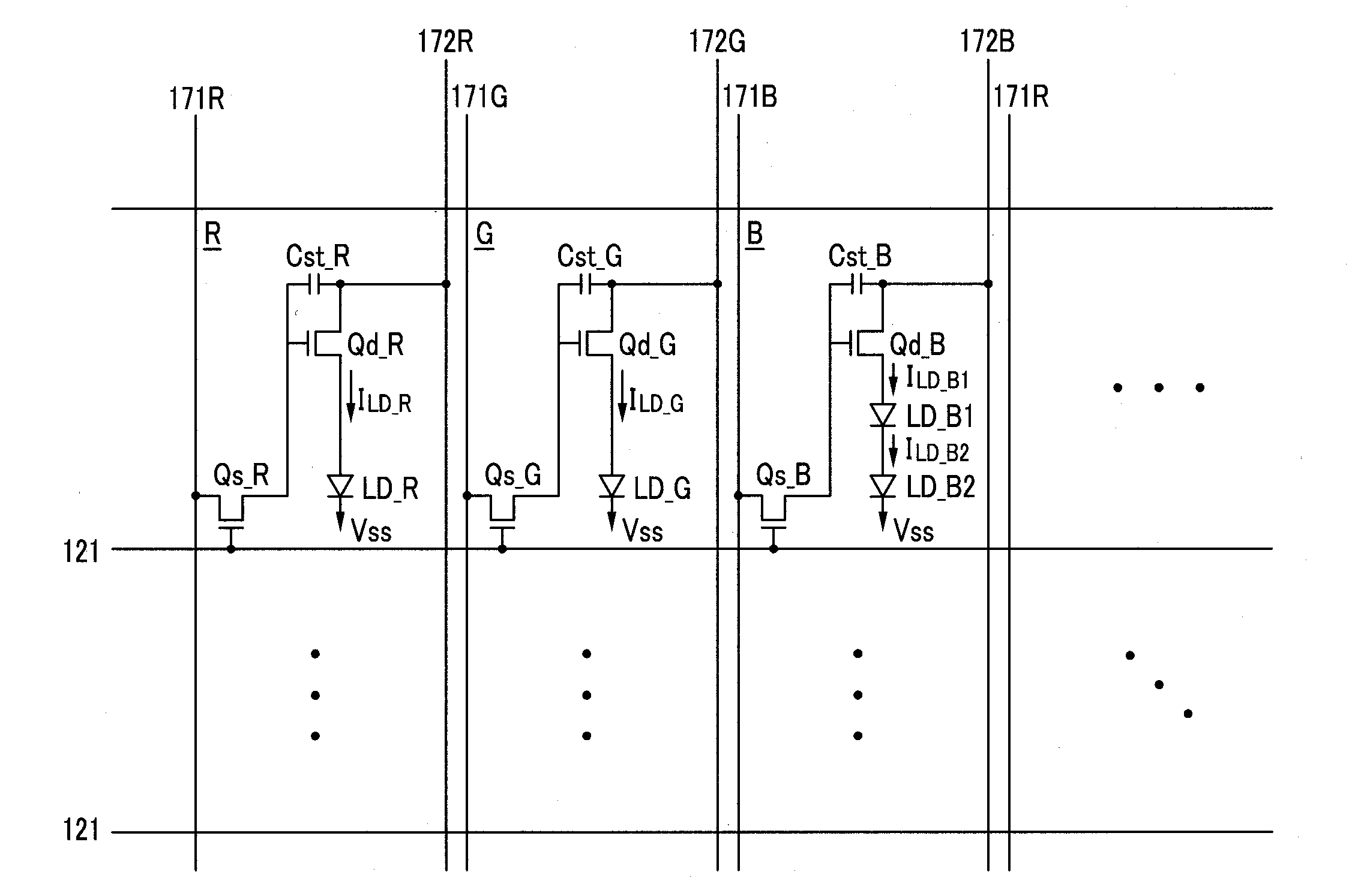
[0100]FIGS. 7 and 8 illustrate another exemplary embodiment of the present invention FIG. 7 is a layout view showing three neighboring pixels corresponding to a region marked by a dotted line in FIG. 1. FIG. 8 is a circuit diagram showing these red, green, and blue pixels of this embodiment.

[0101]In the present embodiment, the driving voltage lines 172R, 172G of the previous embodiment are merged into a common driving voltage line 172RG transmitting the driving voltages to the red pixel R and the green pixel G. The driving voltage line 172RG runs between the red pixel R and the green pixel G. The blue pixel B receives a driving voltage from a driving voltage line 172B. The driving voltage line 172RG is not necessarily at the same driving voltage as the driving voltage line 172B.

[0102]The red pixel R and the green pixel G may be symmetrical with respect to the driving voltage line 172RG. In the other respects, this embodiment is identical to the previous embodim...


PUM


Abstract

In an organic light emitting diode display comprising a first pixel and a second pixel that are associated with respective different colors, each of the first and second pixels being for displaying its associated color, each of the first and second pixels comprises: a first electrode; a second electrode facing the first electrode; and a light emitting member formed between the first electrode and the second electrode; wherein the light emitting member of the first pixel comprises: at least two light-emitting elements for emitting light of the color associated with the first pixel; and a charge generation layer between the at least two light-emitting elements; and wherein the second pixel has fewer light-emitting elements than the first pixel.

Description

CROSS-REFERENCE TO RELATED APPLICATION[0001]This application claims priority to and the benefit of South Korean Patent Application No. 10-2007-0127678 filed in the Korean Intellectual Property Office on Dec. 10, 2007, the entire contents of which are incorporated herein by reference.BACKGROUND AND SUMMARY[0002]The present invention relates to an organic light emitting diode display.[0003]The wide use of personal computers and televisions sets has been accompanied by a demand for lightweight and thin display devices. This demand has been met by flat panel displays such as liquid crystal displays (LCD), which often displaced the heavier and bulkier cathode ray tube displays (CRTs).[0004]However, the LCD is a passive display device, so it may need an additional light source such as backlight. Also, the LCD has various problems such as a slow response time and a narrow viewing angle.[0005]An organic light emitting diode (OLED) display is another type of a flat panel display which has re...

Claims


Application Information

Patent Timeline
IPC IPC(8): G09G3/12H01J1/63
CPCG09G2300/0426G09G2300/0452G09G2300/0809H01L51/5278G09G2320/043H01L27/3211H01L27/3244G09G2300/0819H10K59/35H10K59/12H10K50/19H05B33/02
Inventor KIM, HYO-SEOKPARK, KYONG-TAE
Owner SAMSUNG DISPLAY CO LTD
Why Eureka
Try Eureka