This helps you quickly interpret patents by identifying the three key elements:
Problems solved by technology
Method used
Benefits of technology
Benefits of technology
[0012] The present invention is intended to obviate the above-mentioned problems, and has for its object to obtain a semiconductor pressure sensor in which the damage of bonding wires can be reduced to increase their life time even under an environment in which the temperature and pressure change rapidly and radically.
[0014] According to the semiconductor pressure sensor of the present invention, the damage of the bonding wires can be reduced even under an environment in which the temperature and pressure change rapidly or drastically, and hence the life time of the pressure sensor can be increased.
Problems solved by technology
However, minute gaps or clearances are formed in interfaces between the package and the leads which are formed integral with the package by means of insert molding, so when the diaphragm and the bonding wires are covered with the protective resin portion, air existing in the interfaces is released into the protective resin portion, as a result of which a stress is applied to the bonding wires, thereby causing a fear that the bonding wires might be damaged.
In order to prevent such a situation, a countermeasure is taken in which work to cover the protective resin portion is carried out under a vacuum atmosphere so as to reduce the amount of air confined or trapped in the interfaces, but even in this case, when the diaphragm is subjected to a negative pressure lower than the atmospheric pressure, the air existing in the minute gap expands as air bubbles to invade into the protective resin portion, whereby the protective resin portion and the bonding wires are stressed, and hence there was still a problem that the damage of the bonding wires might be caused.
Here, note that a similar problem was generated by the air that invaded from the outside of the package through small gaps.
Accordingly, even in this case, there was a problem that the bonding wires might be damaged.
Method used
Image
Click on the blue label to locate the original text in one second.
Reading with bidirectional positioning of images and text.
Examples
embodiment 1
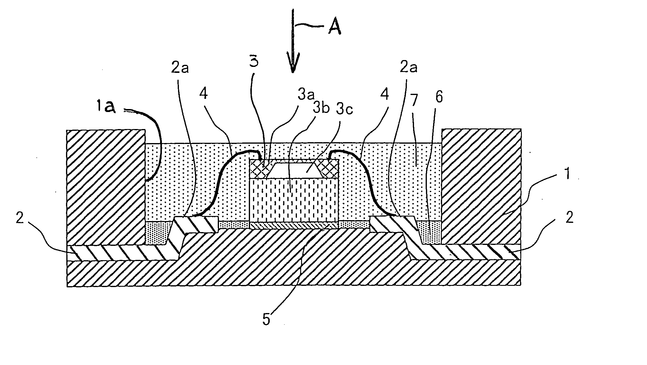
[0023]FIG. 1 is a cross sectional view that shows a semiconductor pressure sensor according to a first embodiment of the present invention.
[0024] In this semiconductor pressure sensor, a concave portion 1a for insulation of a semiconductor chip in the form of a sensor chip 3 is formed in a package 1 made of epoxy resin of a thermosetting property.
[0025] The sensor chip 3 is comprised of a glass seat 3b with a bonding portion 5 bonded to the bottom of the concave portion 1a, and a diaphragm 3a made of a Si material and attached to the glass seat 3b through anode bonding. Formed between the diaphragm 3a and the glass seat 3b is a vacuum chamber 3c which serves as a reference for measured pressure.
[0027] Leads 2 are formed integral with the package 1 by insert molding, and have their one end exposed into the concave portion 1a, and their other end extended from the package 1 to the o...
embodiment 2
[0044]FIG. 5 is a cross sectional view that shows a semiconductor pressure sensor according to a second embodiment of the present invention.
[0045] In this semiconductor pressure sensor, a sensor chip 3 is bonded to the bottom of a concave portion 1a through a first protective resin portion 6.
[0046] The construction of this second embodiment other than the above is similar to that of the first embodiment.
[0047] According to the semiconductor pressure sensor of this embodiment, advantageous effects similar to those of the first embodiment can be achieved, and in addition, the first protective resin portion 6 has not only a function to seal interfaces between leads 2 and a package 1 on the side of the concave portion 1a but also a function to bond the sensor chip 3 to the package 1, whereby a step of applying a bonding material to a bonding portion 5 required in the first embodiment becomes unnecessary and hence assembling efficiency is improved.
embodiment 3
[0048]FIG. 6 is a cross sectional view that shows a semiconductor pressure sensor according to a third embodiment of the present invention.
[0049] In this semiconductor pressure sensor, a processor chip 8, which serves to correct and amplify an electric signal from a sensor chip 3 for detecting pressure, is arranged in a concave portion 1a together with the sensor chip 3.
[0050] The processor chip 8 in the form of a semiconductor chip is bonded to a protruded portion of the bottom of the concave portion 1a through a bonding portion 5.
[0051] In this processor chip 8, too, similar to the sensor chip 3, a plurality of bonding wires 4 are connected at their opposite ends with bonding pads 2a and edges of the processor chip 8 by means of thermo-compression bonding using ultrasonic waves in combination.
[0052] The construction of this third embodiment other than the above is similar to that of the first embodiment, and the same advantageous effects as in the first embodiment can be achie...
PUM
Abstract
A semiconductorpressure sensor can reduce the damage of bonding wires to increase their life time even under an environment in which the temperature and pressure change rapidly and radically. The semiconductorpressure sensor includes a package (1) made of a resin and having a concave portion (1a), a lead (2) formed integral with the package (1) by insert molding, with its one end exposed into the concave portion (1a) and its other end extended from the package (1) to the outside, a sensor chip (3) arranged in the concave portion (1a) for detecting pressure, and a bonding wire (4) electrically connecting the sensor chip (3) and the lead (2) with each other. An interface between the lead (2) and the package (1) on the side of the concave portion (1a) is covered with a first protective resin portion (6) of electrically insulating property, and the bonding wire (4) is covered with a second protective resin portion (7) that is softer than the first protective resin portion (6).
Description
BACKGROUND OF THE INVENTION [0001] 1. Field of the Invention [0002] The present invention relates to a semiconductorpressure sensor for detecting a pressure such as, for example, the pressure in an intake manifold of an internal combustion engine, the internal pressure of a tank, etc [0003] 2. Description of the Related Art [0004] As a general pressure sensing element, there has been known a semiconductor pressure sensor using a piezoresistive effect, for example. [0005] Such a semiconductor pressure sensor is constructed as follows. That is, a seat with a diaphragm bonded thereto is arranged in a concave portion of a package, and a strain gauge formed on the diaphragm serves to catch, as a change in resistance, a strain or distortion of the diaphragm that is caused by a pressure difference between a medium or fluid to be measured and a vacuum chamber defined between the diaphragm and the seat, so that the change in resistance is output as an electric signal to the outside through ...
Claims
Application Information
Patent Timeline
Application Date:The date an application was filed.
Publication Date:The date a patent or application was officially published.
First Publication Date:The earliest publication date of a patent with the same application number.
Issue Date:Publication date of the patent grant document.
PCT Entry Date:The Entry date of PCT National Phase.
Estimated Expiry Date:The statutory expiry date of a patent right according to the Patent Law, and it is the longest term of protection that the patent right can achieve without the termination of the patent right due to other reasons(Term extension factor has been taken into account ).
Invalid Date:Actual expiry date is based on effective date or publication date of legal transaction data of invalid patent.

