Pixel correction system and method for CMOS imagers

Inactive Publication Date: 2009-05-19
STMICROELECTRONICS SRL
View PDF21 Cites 7 Cited by
  • Summary
  • Abstract
  • Description
  • Claims
  • Application Information

AI Technical Summary

Benefits of technology

[0010]The present invention provides a fault tolerant radiation imager such as a CMOS imager. Such image sensor includes circuitry for masking and/or correcting defective pixels during image generation. Masking may involve, in one example, replacing the output of a given pixel with an average of the outputs of surrounding non-faulty pixels. Correction may involve increasing or decreasing the output level from a pixel to be corrected. Thus, while image sensors may be fabricated with some number of faulty pixels, the images produced by such sensors will be superior t

Problems solved by technology

CCD arrays are limited in that all image data is read by shifting analog charge packets from the CCD array interior to the periphery in a pixel-by-pixel manner.
Unfortunately, the pixels of the CCD array are not randomly addressable.
In addition, due to voltage, capacitance, and process constraints, CCD arrays are not well suited to integration at the level possible in CMOS integrated circuits.
This, of course, increases the system's cost.
A persistent problem of both CMOS and CCD image sensor technologies is image degradation due to faulty pixels.
Such faulty pixels arise from processing variations inherent in fabricati

Method used


Image

  • Pixel correction system and method for CMOS imagers
  • Pixel correction system and method for CMOS imagers
  • Pixel correction system and method for CMOS imagers

Examples


Example

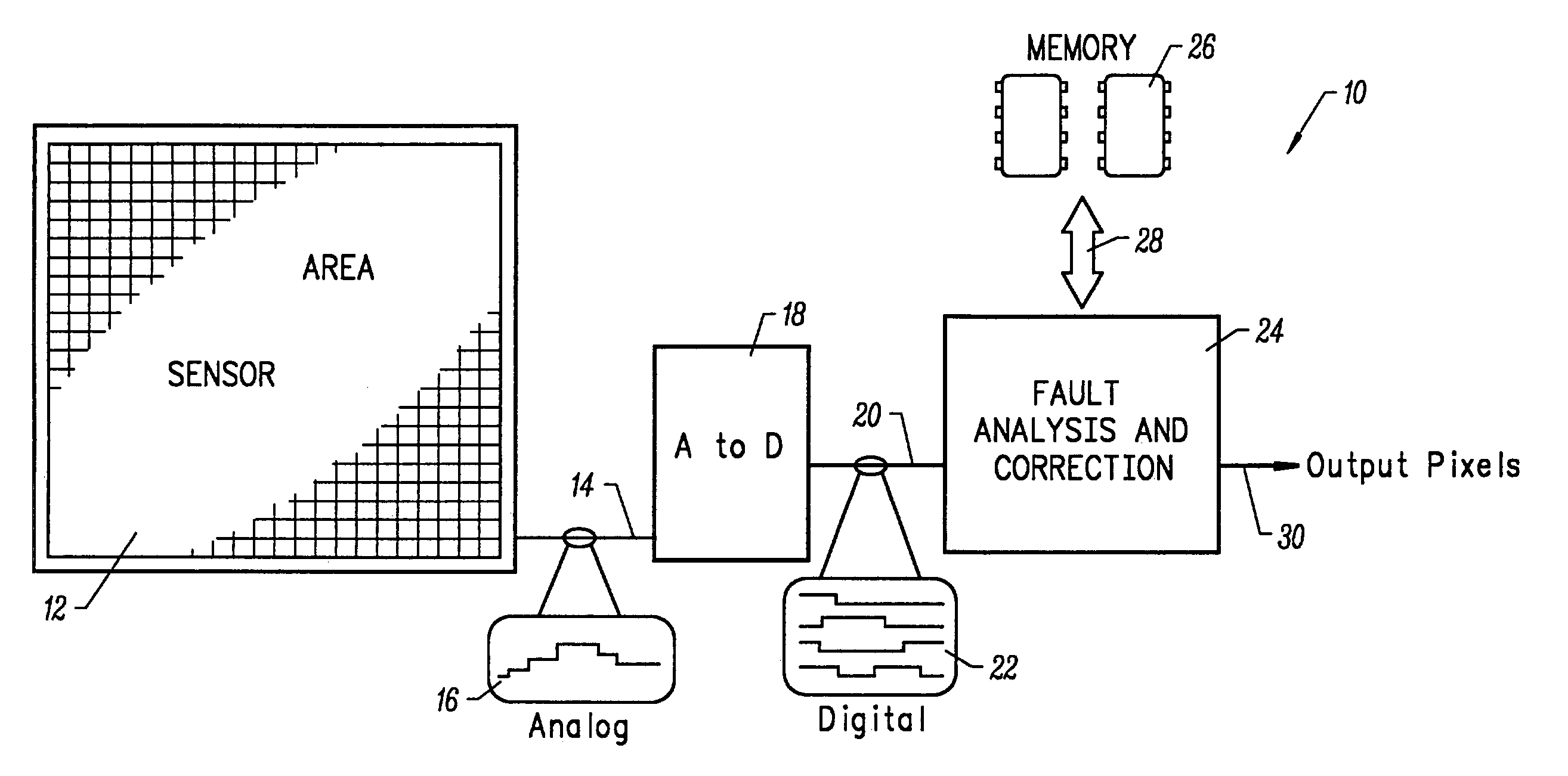
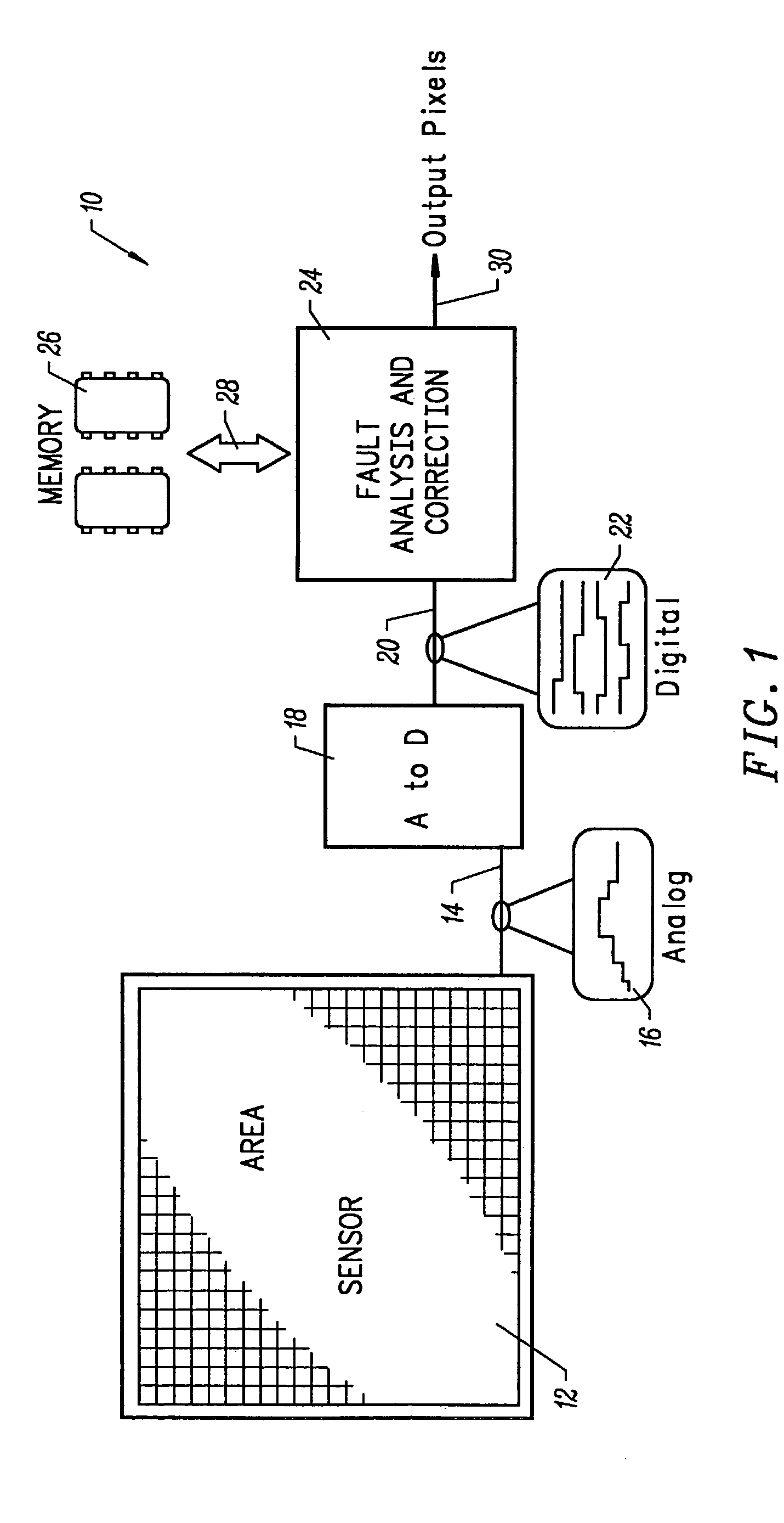
[0032]The invention will be described with reference to certain preferred embodiments set forth below. Specifically, the invention will be described with reference to a particular CMOS sensor employing depletion mode photodiodes. It should be understood that the invention is in no way specifically limited to these embodiments. For example, the methods and systems described herein may be profitably applied to photogate arrays, CCD arrays and virtually any other type of radiation imaging array. Further, while the CMOS photodiode array design presented herein is a “passive” design, the principles of this invention can be applied to other designs such as active pixel designs.

[0033]FIG. 1 presents one preferred system architecture for implementing a CMOS imager in accordance with this invention. Preferably, all elements of the depicted system are implemented on a single integrated circuit chip. The figure presents an imager 10 including four primary elements: a pixel array area sensor 12...


PUM


Abstract

Disclosed is a fault tolerant CMOS image sensor that includes circuitry for identifying defective pixels and masking them during image generation. Masking may involve, in one example, replacing the output of a given pixel with an average of the output of surrounding non-faulty pixels. Thus, while image sensors may be fabricated with some number of faulty pixels, the images produced by such sensors will not have undesirable bright or dark spots. The disclosed sensor includes (a) one or more pixels (active or passive) capable of providing outputs indicative of a quantity of radiation to which each of the one or more pixels has been exposed; and (b) one or more circuit elements electrically coupled to the one or more pixels and configured to identify and correct faulty pixels in the CMOS imager. The one more pixels each include a photodiode diffusion formed in a well and a tap to power or ground also formed in the well. The disclosed sensor also identifies pixels that were initially acceptable but later became defective. The newly defective pixels so identified may then be masked to thereby increase the CMOS detector lifetime.

Description

[0001]This is a Divisional application of prior application Ser. No. 08 / 964,763 filed on Nov. 5, 1997 now U.S. Pat. No. 6,618,084, the disclosure of which is incorporated herein by reference.BACKGROUND OF THE INVENTION[0002]The present invention relates to an integrated circuit architecture for CMOS imagers. More specifically, the present invention relates to methods and apparatus for masking or correcting faults in individual pixels of CMOS imagers.[0003]CMOS image sensors are now becoming competitive with charge coupled device (“CCD”) array image sensors. Potential applications include digital cameras, night time driving displays for automobiles, and computer peripherals for document capture and visual communications.[0004]Since the 1970s, CCD arrays have dominated the electronic image sensor market. They have outperformed CMOS array sensors in most areas, including quantum efficiency, optical fill factor (the fraction of a pixel used for detection), charge transfer efficiency, re...

Claims


Application Information

Patent Timeline
IPC IPC(8): H04N9/64H04N5/367H01L27/146H04N5/374
CPCH04N5/367H04N5/374H04N25/68H04N25/76
Inventor RAMBALDI, ROBERTOTARTAGNI, MARCOKRAMER, ALAN H.
Owner STMICROELECTRONICS SRL
Why Eureka
Try Eureka