Method for fabricating light emitting diode chip

Active Publication Date: 2010-01-21
LEXTAR ELECTRONICS CORP
View PDF6 Cites 21 Cited by
  • Summary
  • Abstract
  • Description
  • Claims
  • Application Information

AI Technical Summary

Benefits of technology

[0012]In light of the foregoing, the present invention provides a method for fabricating a light emitting diode chip. The method applies a half-tone mask process, a gray-tone mask process or a multi-tone mask process, a

Problems solved by technology

Since each of the masks is rather costly, the fabrication cost and the

Method used


Image

  • Method for fabricating light emitting diode chip
  • Method for fabricating light emitting diode chip
  • Method for fabricating light emitting diode chip

Examples


first embodiment

The First Embodiment

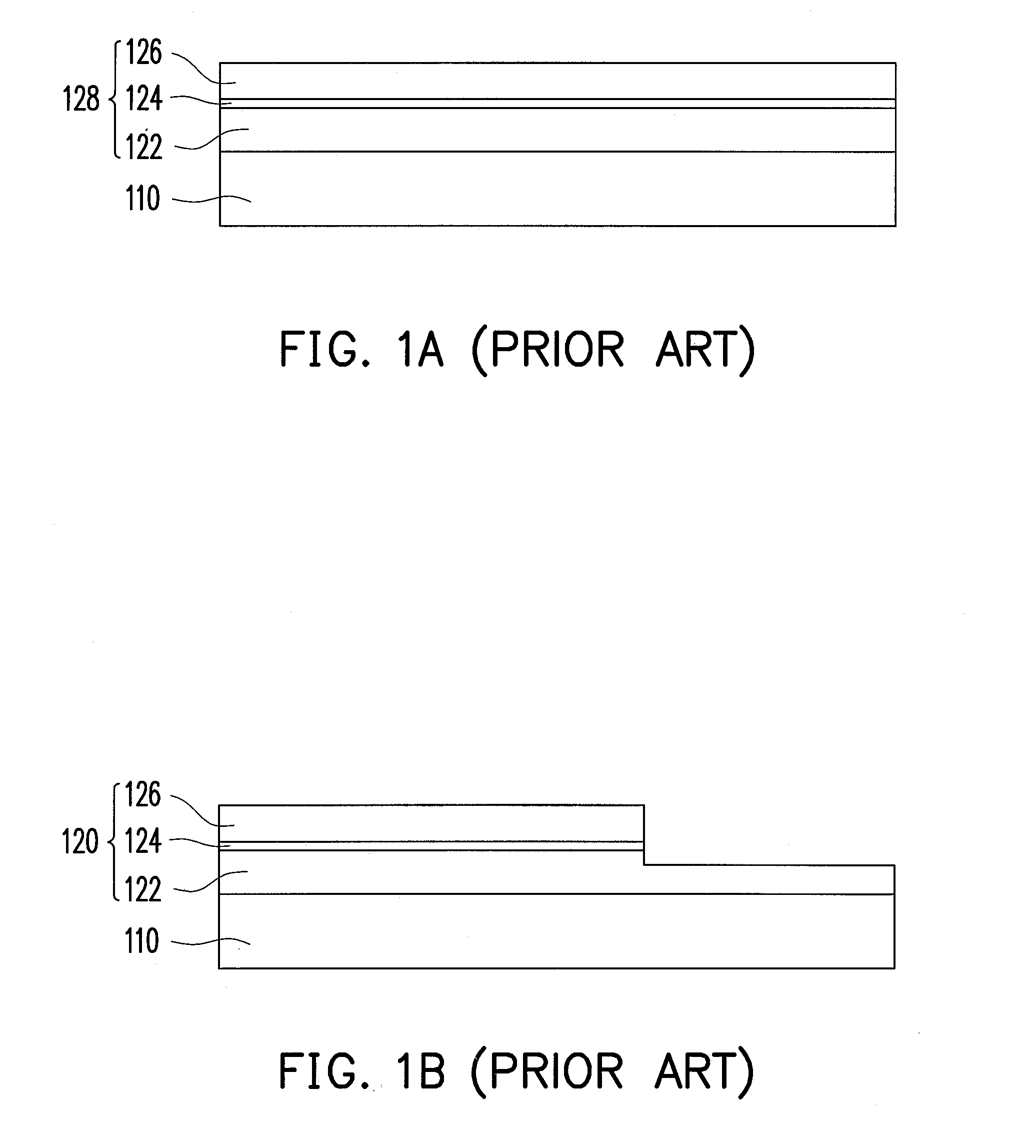
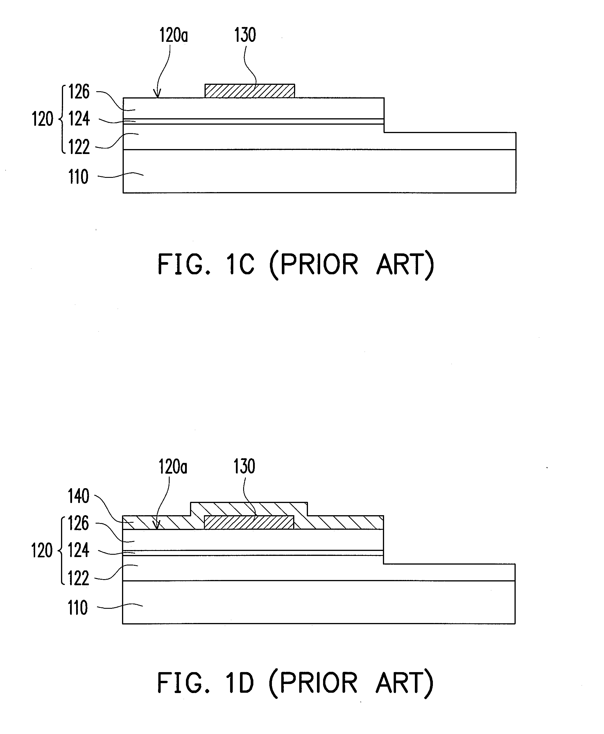
[0070]FIGS. 2A through 2I show a schematic flowchart of fabricating a light emitting diode chip according to the first embodiment of the present invention. First, a first type semiconductor material layer 222, a light emitting material layer 224 and a second type semiconductor material layer 226 are sequentially formed on a substrate 210 to further form a semiconductor layer 228, as shown by FIG. 2A. The semiconductor layer 228 is formed, for example, by a metal organic chemical vapor deposition (MOCVD) process, a molecular beam epitaxial (MBE) process, or other suitable epitaxial growth processes, to sequentially form the said material layers 222, 224 and 226 on the substrate 210. The present embodiment is exemplified by an MOCVD process as an example of embodiment but not limited thereto. According to the present embodiment, a material of the substrate 210 is aluminum oxide with good transmittance, for example. Furthermore, to give some examples, a material sel...

second embodiment

The Second Embodiment

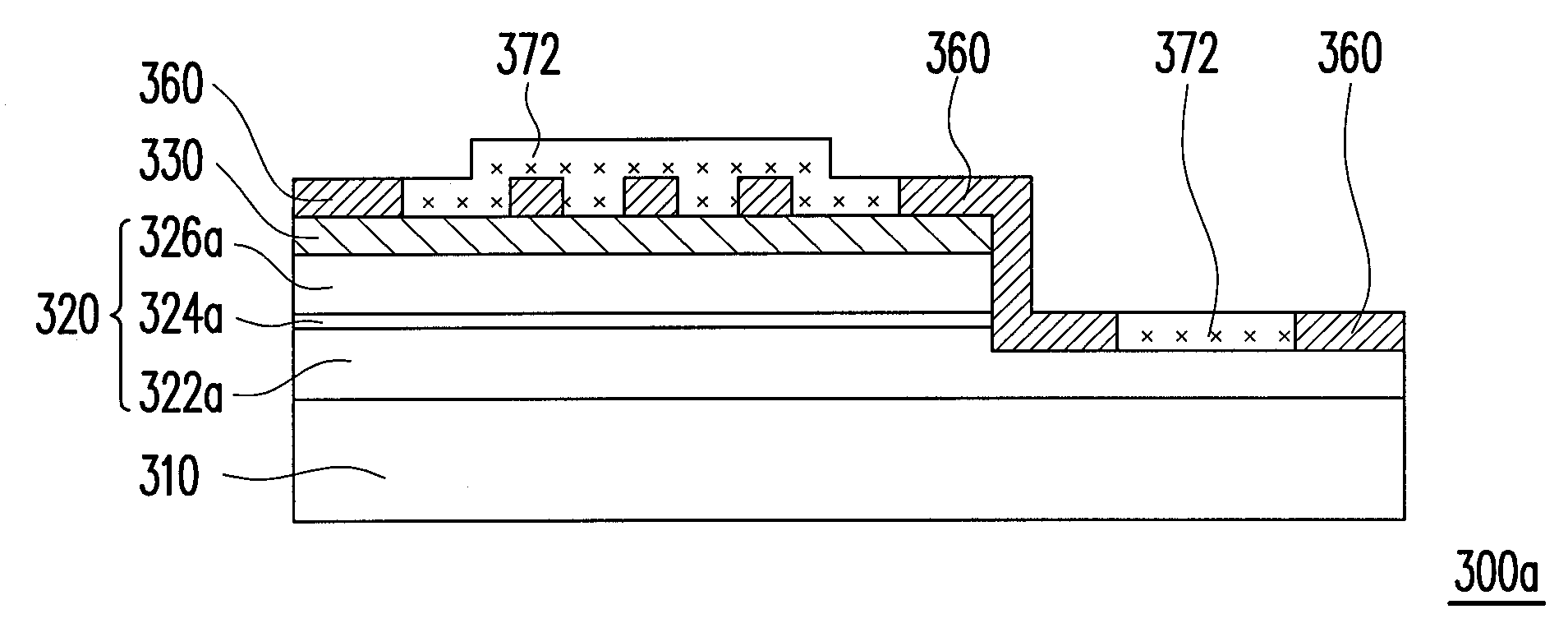
[0100]FIGS. 6A through 6H show a schematic flowchart of fabricating a light emitting diode chip according to the second embodiment of the present invention. First, a first type semiconductor material layer 322, a light emitting material layer 324, a second type semiconductor material layer 326 and a conductive layer 332 are sequentially formed on a substrate 310 to further form a semiconductor layer 328 and the conductive layer 332 on the semiconductor layer 328 respectively, as shown by FIG. 6A. The semiconductor layer 328 and the conductive layer 332 formed on the semiconductor layer 328 are used the following methods, for example, MOCVD, MBE, evaporation, sputtering or other suitable epitaxial growth processes to sequentially form the material layers 322, 324, 326 and the conductive layer 332 on the substrate 310. In the present embodiment, an MOCVD process is used as an example for the mode of embodiment, but the present embodiment is not limited thereto. Ac...

third embodiment

The Third Embodiment

[0117]FIGS. 8A through 8F show a schematic flowchart of fabricating a light emitting diode chip according to the third embodiment of the present invention. First, a first type semiconductor material layer 422, a light emitting material layer 424, a second type semiconductor material layer 426 and a conductive layer 432 are sequentially formed on a substrate 410 to further form a semiconductor layer 428 and a conductive layer 432 on the semiconductor layer 428 respectively, as shown by FIG. 8A. According to the present embodiment, the semiconductor layer 428 and the conductive layer 432 thereon are formed, for example, by MOCVD, MBE, evaporation, sputtering or other suitable epitaxial growth processes to sequentially form the material layers 422, 424, 426 and the conductive layer 432 on the substrate 410. The present embodiment is exemplified by an MOCVD process as an example for embodiment but not limited thereto. According to the present embodiment, the substrat...


PUM


Abstract

A method for fabricating a light emitting diode chip is provided. In the method, a half-tone mask process, a gray-tone mask process or a multi-tone mask process is applied and combined with a lift-off process to further reduce process steps of the light emitting diode chip. In the present invention, some components may also be simultaneously formed by an identical process to reduce the process steps of the light emitting diode chip. Consequently, the fabricating method of the light emitting diode provided in the present invention reduces the cost and time for the fabrication of the light emitting diode.

Description

CROSS-REFERENCE TO RELATED APPLICATION[0001]This application claims the priority benefit of Taiwan application serial no. 97127462, filed on Jul. 18, 2008. The entirety of the above-mentioned patent application is hereby incorporated by reference herein and made a part of specification.BACKGROUND OF THE INVENTION[0002]1. Field of the Invention[0003]The present invention relates to a method for fabricating a chip, and more particularly to a method for fabricating a light emitting diode chip.[0004]2. Description of Related Art[0005]FIGS. 1A through 1F show a fabrication flowchart of a conventional light emitting diode chip. First, a first type semiconductor material layer 122, a light emitting material layer 124 and a second type semiconductor material layer 126 are sequentially formed on a substrate 110 to further form a semiconductor layer 128, as shown by FIG. 1A. A method for forming the semiconductor layer 128 is, for example, a chemical vapor deposition (CVD) process, during whi...

Claims


Application Information

Patent Timeline
IPC IPC(8): H01L21/00
CPCH01L33/44H01L33/387Y10S438/951
Inventor FANG, KUO-LUNGWENG, CHIEN-SENCHAO, CHIH-WEI
Owner LEXTAR ELECTRONICS CORP
Why Eureka
Try Eureka