Optical waveguide, method of manufacturing the same and optical communication module

a technology of optical communication module and optical waveguide, which is applied in the direction of optical waveguide light guide, instruments, optics, etc., can solve the problems of insufficient assurance of the difference in refractive index between the core layer and the cladding layer, the precision of the resultant core diameter, and the cost of the direct exposure method in (2) and (3), so as to improve the manufacturing efficiency and the effect of simple method and low cos

Inactive Publication Date: 2007-12-20
FUJIFILM BUSINESS INNOVATION CORP
View PDF5 Cites 35 Cited by
  • Summary
  • Abstract
  • Description
  • Claims
  • Application Information

AI Technical Summary

Benefits of technology

[0012]An objection of the present invention is to provide a method of manufacturing an optical waveguide having the electric wire, capable of being cheap cost and improving the manufacturing efficiency by simple method.(1) According to a first aspect of the present invention, an optical waveguide includes: a lower substrate; a waveguide core that is formed on the lower substrate; a clad that is formed to surround a periphery of the waveguide core; and an upper substrate that is opposed to the lower substrate, wherein the waveguide cores, the lower substrate and the upper substrate surround a cavity extended along the waveguide core.
[0013]According to this configuration, when the optical waveguide is bent, a deformation caused due to a distortion, a curvature, etc. can be absorbed and reduced by the cavity, and thus a flexibility of the optical waveguide can be increased irrespective of the material of the optical waveguide. A utility efficiency of materials can be enhanced tremendously, and also a weight reduction of the optical waveguide can be attained.

Problems solved by technology

However, the selective polymerization method in (1) has a problem with the gluing of the films.
The RIE method in (2) and the direct exposure method in (3) need high cost because such methods employ the photolithography.
The injection molding method in (4) has a problem about a precision of the resultant core diameter.
The photo bleaching method in (5) has such a problem that a difference in refractive indexes between the core layer and the cladding layer cannot be sufficiently ensured.
The RIE method in (2) and the direct exposure method in (3) can be listed as the practical manufacturing method, but these methods have a problem with a production cost as described above.
All manufacturing methods in (1) to (5) needs a wide area, and are not practically fit for forming the polymer optical waveguide on the flexible plastic substrate.
In addition, when the electric wiring pattern and optical interconnection pattern (core) are manufactured, complicate and many step is needed due to manufacturing by various thin film forming process, for example, patterning, exposure and development, and etching, or so like.
Therefore, there are problems that fabrication yield easily gets worse and production cost sores.

Method used


Image

  • Optical waveguide, method of manufacturing the same and optical communication module
  • Optical waveguide, method of manufacturing the same and optical communication module
  • Optical waveguide, method of manufacturing the same and optical communication module

Examples


first embodiment

(Configuration of the Optical Waveguide)

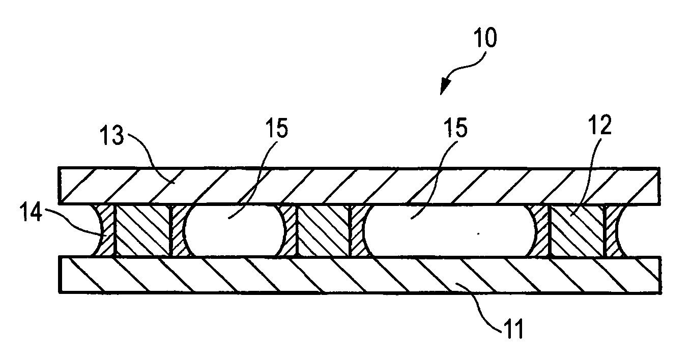
[0023]FIG. 1 is a sectional view showing schematically a configurative example of an optical waveguide according to a first embodiment of the present invention.

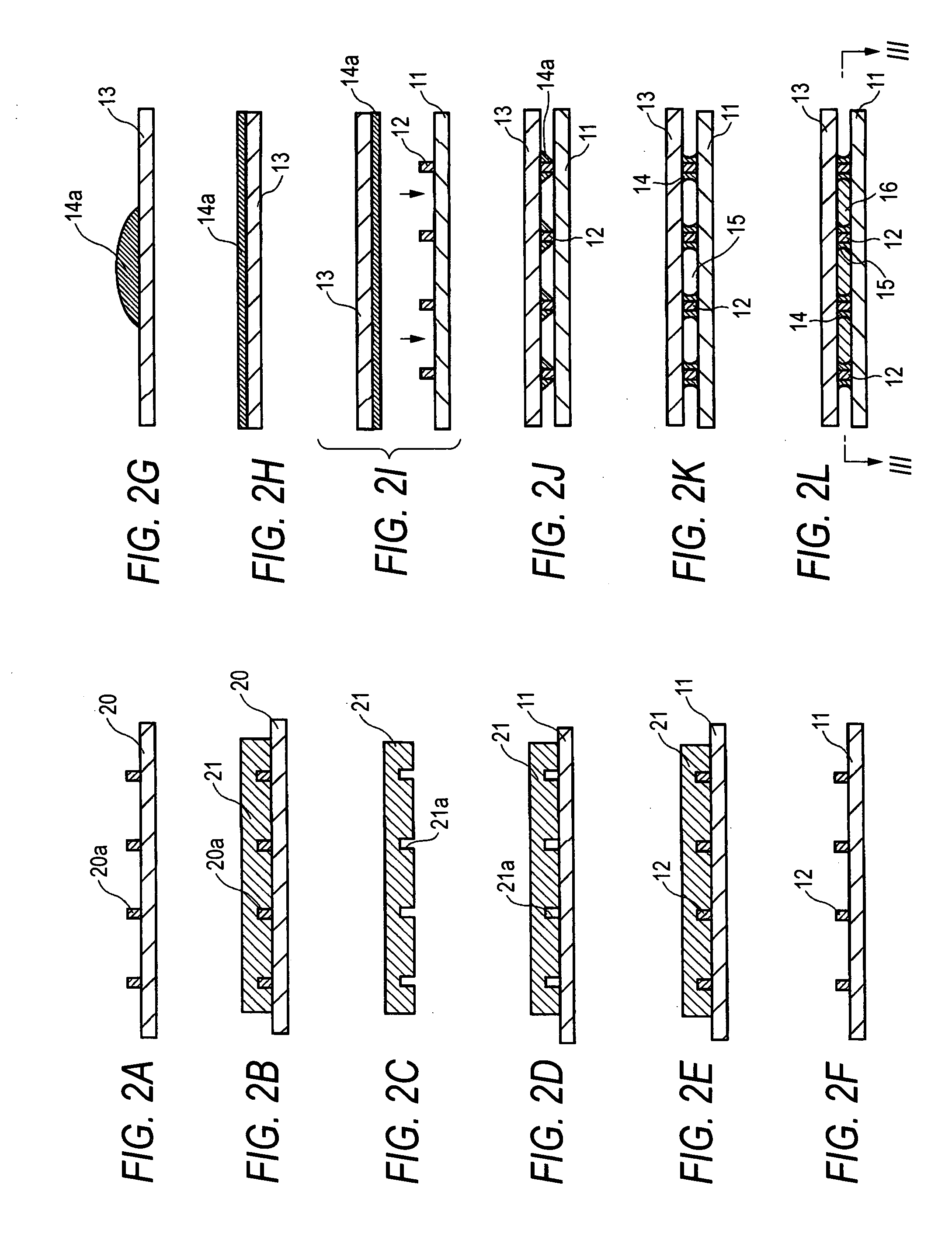
[0024]In FIG. 1, a reference symbol 10 denotes a configurative example of the optical waveguide. As shown in FIG. 1, a basic configuration of the optical waveguide 10 includes a lower substrate 11 serving as a cladding layer, waveguide cores 12 formed on the lower substrate 11, an upper substrate 13 opposed to the lower substrate 11 to put the waveguide cores 12 between them and serving as a cladding layer, thin film clads 14 formed on side surfaces of the waveguide cores 12 respectively, and cavities 15 formed between the opposing clads 14. The lower substrate 11 and the upper substrate 13 are formed of a film member, a sheet member, or the like, for example, to have a rectangular shape. The waveguide cores 12 and the cavities 15 are formed to have an array structure in which they are ...

second embodiment

(Configuration of Optical Communication Module)

[0044]FIG. 4 shows a configurative example of an optical communication module according to a second embodiment of the present invention. FIG. 4 is a conceptual view showing a configuration of the optical communication module. In FIG. 4, the same member names and the same reference symbols are affixed to the substantially same members as those in the first embodiment. Therefore, detailed explanation regarding these members will be omitted herein.

[0045]In FIG. 4, a reference numeral 30 denotes an optical communication module equipped with the flexible polymer optical waveguide 10 as the first embodiment. This optical communication module 30 has the array structure in which the waveguide cores 12 and the cavities 15 constituting the optical wiring pattern are extended mutually. The curable resin shown in FIG. 3B is filled / cured in the opening end portions of the cavities 15. Alight emitting portion consisting of a single light emitting ele...

third embodiment

(Configuration of Optical Communication Module)

[0047]FIG. 5 shows a configurative example of an optical communication module according to a second embodiment of the present invention. FIG. 5 is a conceptual view showing a configuration of the optical communication module. In FIG. 5, the same member names and the same reference symbols are affixed to the substantially same members as those in the first embodiment. Therefore, detailed explanation regarding these members and constructions will be omitted herein.

[0048]In FIG. 5, a reference symbol 10 denotes a configurative example of the optical waveguide having the electric wire. As shown in FIG. 5, a basic configuration of the optical waveguide 10 includes a lower substrate 11 serving as a cladding layer, waveguide cores 12 formed on the lower substrate 11, an upper substrate 13 opposed to the lower substrate 11 to put the waveguide cores 12 between them and serving as a cladding layer, thin film clads 14 formed on side surfaces of t...


PUM


Abstract

An optical waveguide includes: a lower substrate; a waveguide core that is formed on the lower substrate; a clad that is formed to surround a periphery of the waveguide core; and an upper substrate that is opposed to the lower substrate, wherein the waveguide cores, the lower substrate and the upper substrate surround a cavity extended along the waveguide core.

Description

BACKGROUND[0001]1. Technical Field[0002]The present invention relates to an optical waveguide and a method of manufacturing the same, and an optical communication module and, more particularly, an optical waveguide and a method of manufacturing the same, and an optical communication module, capable of making sure of a flexibility without change of the material, achieving a weight reduction, being cheap price, improving the manufacturing efficiency by simple method.[0003]2. Related Art[0004]As an example of the method of manufacturing the polymer optical waveguide in the prior art, various manufacturing methods such as[0005](1) the method of impregnating a film with a monomer, exposing selectively a core portion to change a refractive index, and gluing films together (selective polymerization method),[0006](2) the method of coating a core layer and a cladding layer and then forming a cladding portion by using the reactive ion etching (RIE method),[0007](3) the method of exposing / deve...

Claims


Application Information

Patent Timeline
Patent Type & Authority Applications(United States)
IPC IPC(8): G02B6/10
CPCG02B6/138G02B6/43G02B6/4214
Inventor FUJII, AKIRASUZUKI, TOSHIHIKOSHIMIZU, KEISHIYATSUDA, KAZUTOSHIOHTSU, SHIGEMIAKUTSU, EIICHI
Owner FUJIFILM BUSINESS INNOVATION CORP
Why Eureka
Try Eureka