Semiconductor device and method of fabricating the same
- Summary
- Abstract
- Description
- Claims
- Application Information
AI Technical Summary
Benefits of technology
Problems solved by technology
Method used
Image
Examples
first embodiment
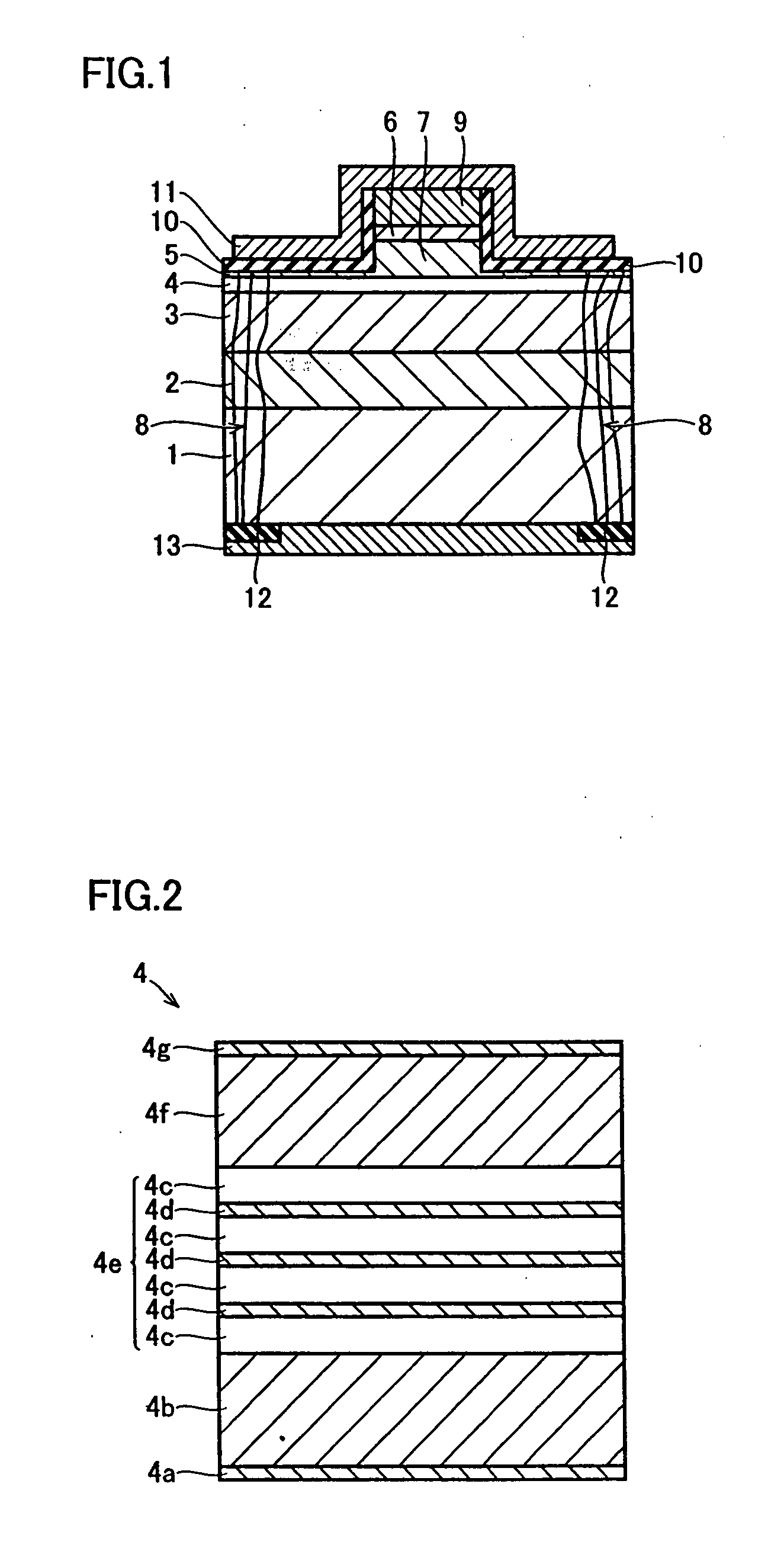
[0082] The structure of a nitride-based semiconductor laser device according to a first embodiment of the present invention is described with reference to FIGS. 1 and 2.
[0083] In the nitride-based semiconductor laser device according to the first embodiment, an n-type layer 2 having a thickness of about 100 nm and consisting of n-type GaN doped with Si having an atomic density of about 5×1018 cm−3 is formed on the (0001) plane of an n-type GaN substrate 1 of a wurtzite structure having a thickness of about 100 μm and doped with oxygen having a carrier concentration of about 5×1018 cm−3, as shown in FIG. 1. An n-type cladding layer 3 having a thickness of about 400 nm and consisting of n-type Al0.05Ga0.95N doped with Si having an atomic density of about 5×1018 cm−3 and a carrier concentration of about 5×1018 cm−3 is formed on the n-type layer 2. The n-type GaN substrate 1 is an example of the “substrate” or the “nitride-based semiconductor substrate” in the present invention, and th...
second embodiment
[0108] Referring to FIG. 13, prescribed regions of ends of an n-type GaN substrate 1 and nitride-based semiconductor layers 2 to 5 are removed in a nitride-based semiconductor laser device according to a second embodiment of the present invention dissimilarly to the aforementioned first embodiment. Therefore, the nitride-based semiconductor laser device is provided with no regions 8 having concentrated dislocations dissimilarly to the first embodiment shown in FIG. 1. An n-side electrode 33 consisting of an Al layer having a thickness of about 10 nm, a Pt layer having a thickness of about 20 nm and an Au layer having a thickness of about 300 nm successively from the side closer to the back surface of the n-type GaN substrate 1 is formed on the back surface of the n-type GaN substrate 1 to be in contact with the overall back surface of the n-type GaN substrate 1. The n-side electrode 33 is an example of the “back electrode” in the present invention. The remaining structure of the sec...
third embodiment
[0114] Referring to FIGS. 16 and 17, a third embodiment of the present invention is applied to a light-emitting diode device, dissimilarly to the aforementioned first embodiment.
[0115] According to the third embodiment, an n-type cladding layer 52 having a thickness of about 5 μm and consisting of n-type GaN doped with Si is formed on an n-type GaN substrate 1, as shown in FIG. 16. The n-type cladding layer 52 is an example of the “semiconductor element layer” in the present invention.
[0116] An emission layer 53 is formed on the n-type cladding layer 52. As shown in FIG. 17, this emission layer 53 is constituted of an MQW active layer 53c formed by alternately stacking six barrier layers 53a of undoped GaN each having a thickness of about 5 nm and five well layers 53b of undoped In0.35Ga0.65N each having a thickness of about 5 nm and a protective layer 53d of undoped GaN having a thickness of about 10 nm. The emission layer 53 is an example of the “semiconductor element layer” in ...
PUM
 Abstract
Description
Claims
Application Information


