Film adhesion device and film adhesion method

a film adhesion and film technology, applied in mechanical control devices, paper/cardboard containers, instruments, etc., can solve the problems of poor yield, high risk of pin holes and so on, and high film thickness, so as to minimize the effect of the lower layer portion

Inactive Publication Date: 2007-12-27
TEIKOKU TAPING SYST
View PDF6 Cites 7 Cited by
  • Summary
  • Abstract
  • Description
  • Claims
  • Application Information

AI Technical Summary

Benefits of technology

[0009]The present inventor has discovered that by minimizing the effect on the lower layer portion when a large number of films (particularly photoresist films) constituted by a thin and flexible material are mechanically adhered, another film can be laminated onto the first layer film, and as a result, a high film thickness can be achieved by laminating a large number of layers using a pre-existing thick material rather than a high film thickness material.

Problems solved by technology

However, when photoresist is applied using a roll coater method in the conventional structure forming method described above, pin holes and so on are likely to form when the coating film thickness is reduced, and when the coating film thickness is increased, waves (indicated by the virtual lines in FIG. 17) and so on are likely to form.
When the photoresist is applied using a spray method, the coating amount becomes unstable when a coating device is driven and stopped, and hence the yield is poor.
Therefore, with the conventional structure forming method described above, it is difficult to form a structure having an extremely thin film thickness while securing a predetermined thickness precision (less than 5% or the like, for example).
Also, an extremely high degree of precision (for example, thickness precision, variation, impurity concentration, and so on) is required of the material constituting the structure, and it is technically difficult to manufacture a structure having a high film thickness.

Method used


Image

  • Film adhesion device and film adhesion method
  • Film adhesion device and film adhesion method
  • Film adhesion device and film adhesion method

Examples


working example

[0079]A working example of the present invention will now be described with reference to the drawings.

(1) Structure of Film Adhesion Device

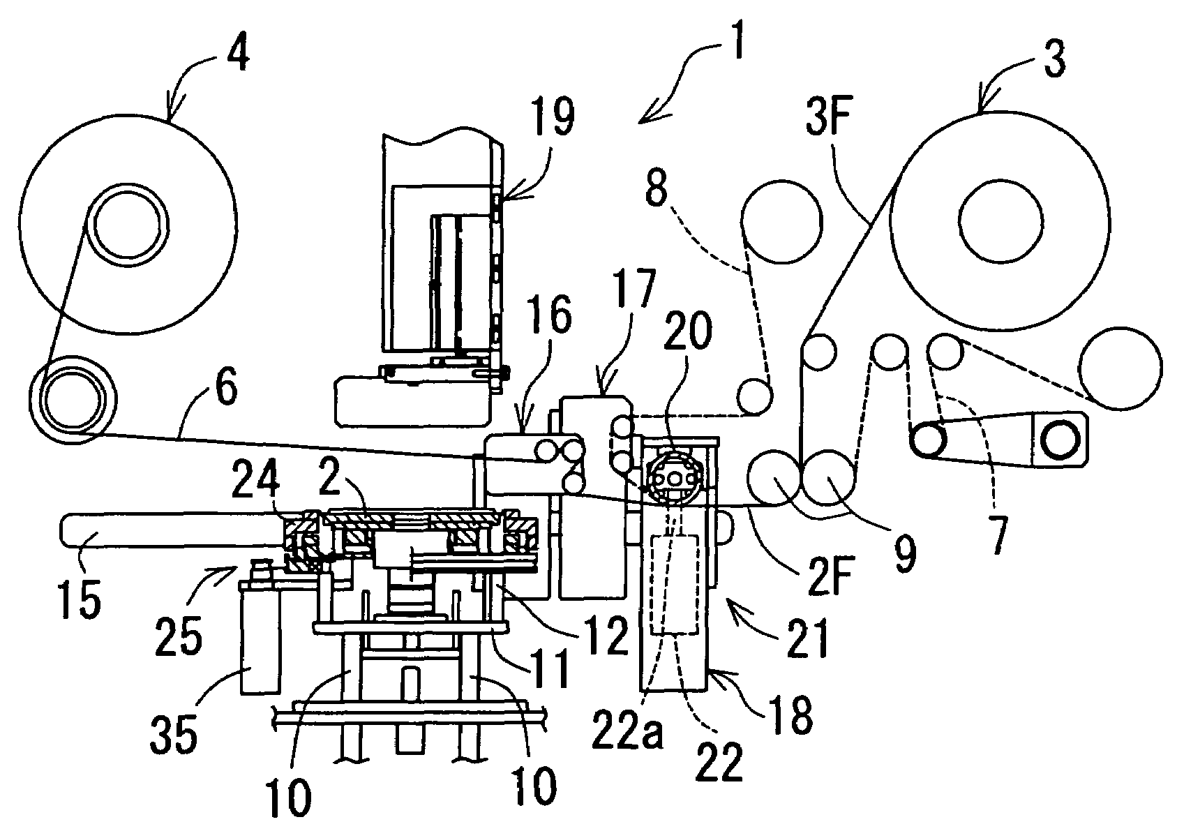
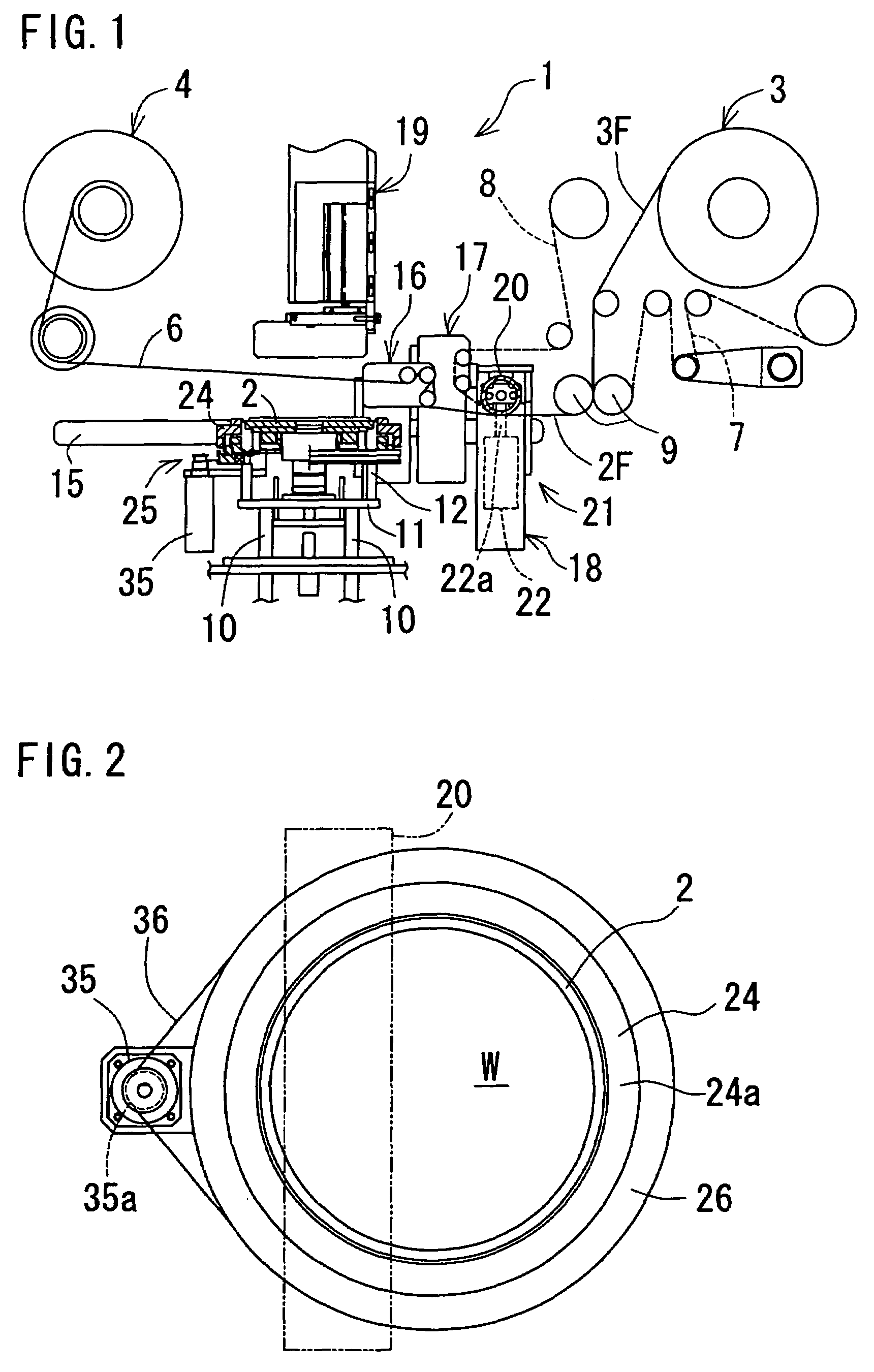
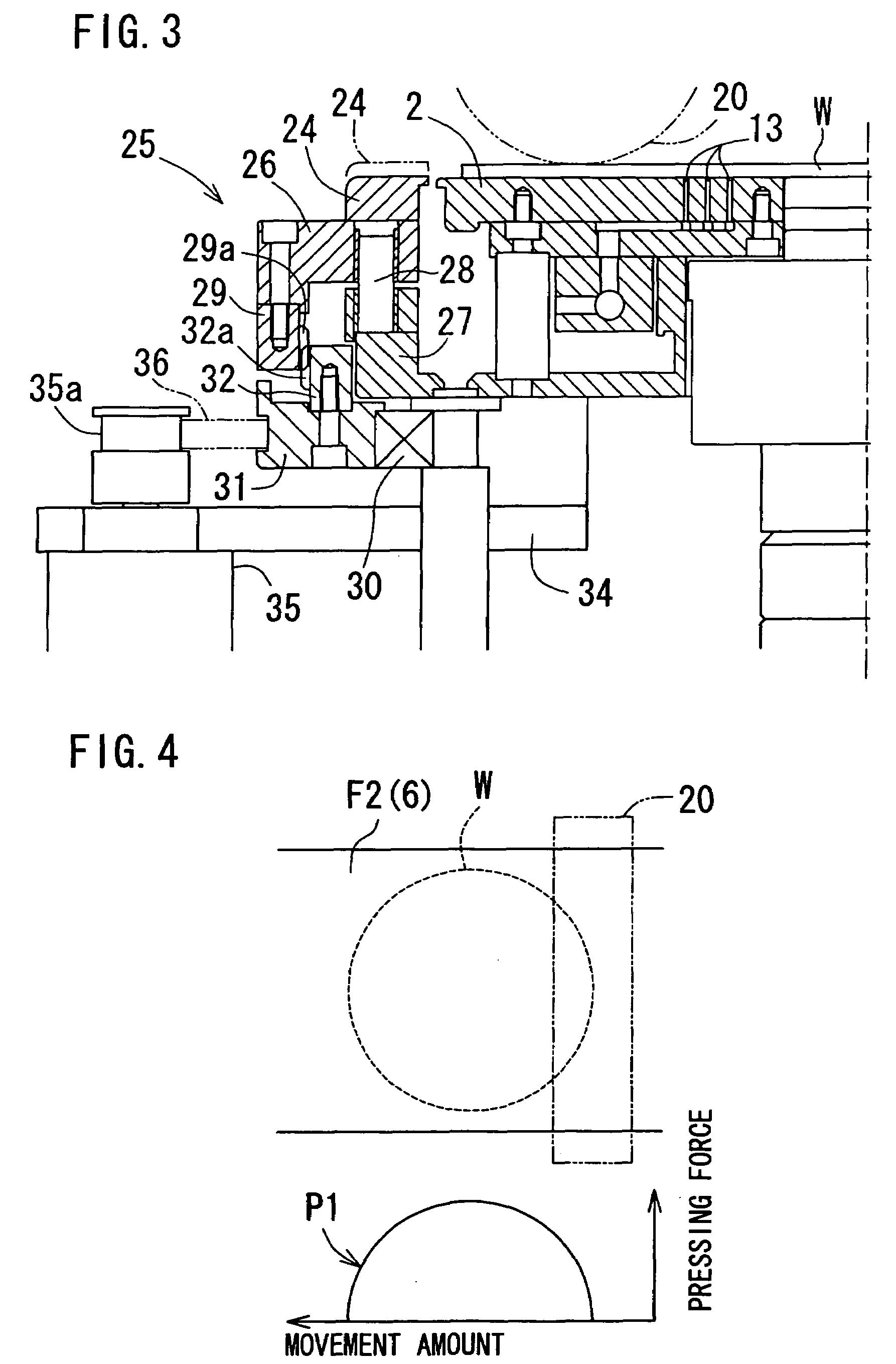
[0080]As shown in FIGS. 1 and 2, a film adhesion device 1 according to this working example includes a disc-shaped table 2 carrying a circular plane-form semiconductor wafer W. A film supply portion 3 and a winding portion 4 forming a pair are disposed at a predetermined interval diagonally above the table 2. A three-layer film F3 is supplied from the film supply portion 3. The three-layer film F3 is constituted by a photoresist film 6 having a heat-sensitive adhesive property with a carrier film 7 laminated onto one surface thereof and a reinforcing film 8 laminated onto the other surface thereof. The carrier film 7 is peeled away from the three-layer film F3 by a pinch roller 9 such that the three-layer film F3 becomes a two-layer film F2. The two-layer film F2 is pressed onto, and thereby adhered to, the surface of the semiconductor wafer W, w...


PUM

PropertyMeasurementUnit
thicknessaaaaaaaaaa
thicknessaaaaaaaaaa
thicknessaaaaaaaaaa

Abstract

A film adhesion device includes a table carrying a semiconductor wafer, a pressing member (pressing roller) which presses a film (photoresist film) onto a surface side of the semiconductor wafer placed on the table, a bumper member provided on an outer peripheral side of the table and including a contact surface which is contacted by the pressing member when the pressing member presses the film, and an elevating support mechanism which supports the bumper member elevatably and positions the bumper member at a predetermined height level.

Description

[0001]The disclosure of Japanese Patent Application No. JP-A-2006-171893 filed on Jun. 21, 2006 including the specification, drawings and abstract is incorporated herein by reference in its entirety.BACKGROUND OF THE INVENTION[0002]1. Field of the Invention[0003]The present invention relates to a film adhesion device and a film adhesion method, and more particularly to a film adhesion device and film adhesion method with which a structure having an extremely thin film thickness and a high film thickness can be formed with good yield and excellent thickness precision on a semiconductor wafer.[0004]2. Description of the Related Art[0005]In recent years, microdevices such as microsensors, microactuators, and optical switches formed by integrating minute elements that are created using semiconductor microprocessing techniques have become known as Micro Electro Mechanical Systems (MEMS).[0006]In these microsensors and so on, a structure (for example, a hollow structure or the like) may b...

Claims


Application Information

Patent Timeline
Patent Type & Authority Applications(United States)
IPC IPC(8): B32B37/00B32B41/00
CPCB32B37/0046B32B2457/14H01L21/67132Y10T156/1082H01L2221/68327Y10T156/1052Y10T156/10H01L21/6836
Inventor LEE, MASAHIRO
Owner TEIKOKU TAPING SYST
Why Eureka
Try Eureka