Semiconductor device and method of manufacturing the same

Inactive Publication Date: 2005-09-13
RENESAS ELECTRONICS CORP
View PDF8 Cites 9 Cited by
  • Summary
  • Abstract
  • Description
  • Claims
  • Application Information

AI Technical Summary

Benefits of technology

[0005]An object of the present invention to provide a semiconductor device in which the occurrence of leak current is suppressed

Problems solved by technology

In this conjunction, it is noted that such thickness of the gate insulation film as mentioned above will give rise to occurrence of a tunnel current of unignorable magnitude.
However, in the present state of the art, when the se

Method used


Image

  • Semiconductor device and method of manufacturing the same
  • Semiconductor device and method of manufacturing the same
  • Semiconductor device and method of manufacturing the same

Examples


first embodiment

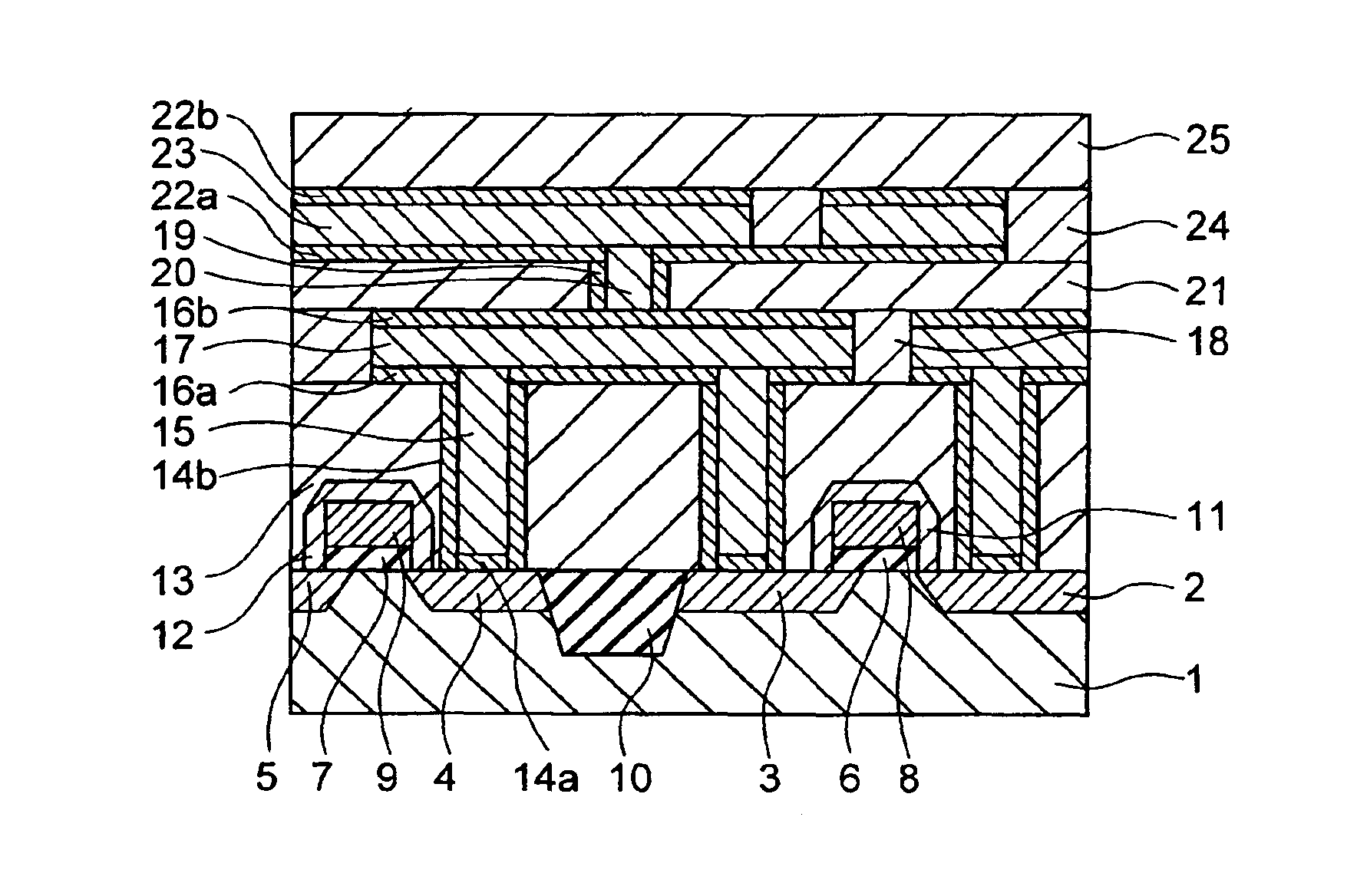
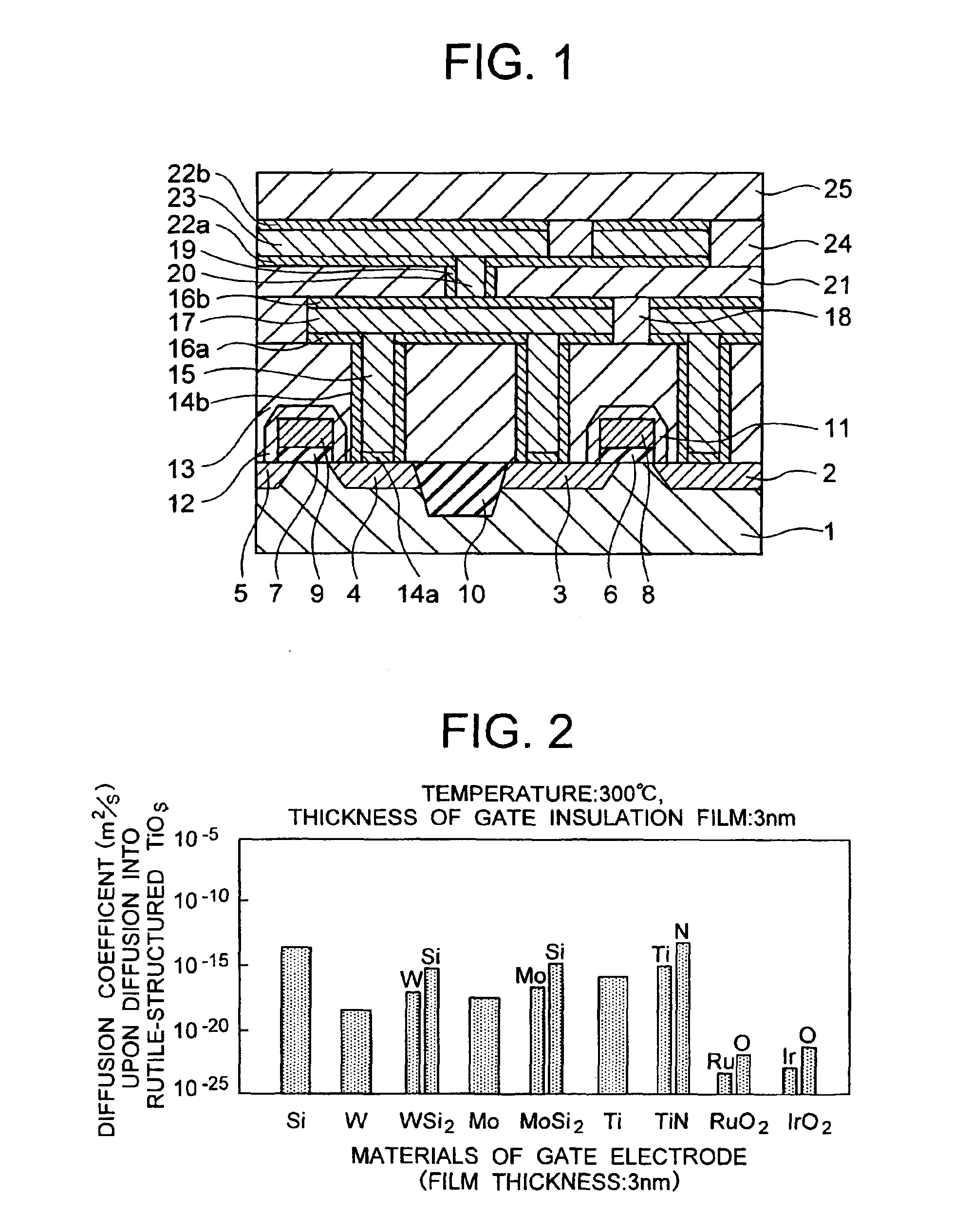
[0039]In the following, typical embodiments of the present invention will be described in detail by reference to the drawings. FIG. 1 is a sectional view showing schematically a structure of a major portion in the semiconductor device according to the present invention.

[0040]Referring to FIG. 1, the semiconductor device according to the first embodiment of the invention is implemented in a structure of the MOS transistor. In this semiconductor device, diffusion layers 2, 3, 4 and 5 are formed on a silicon substrate 1, and gate insulation films 6 and 7 and gate electrodes 8 and 9 are deposited on these diffusion layers.

[0041]With a view to satisfying the requirement for miniaturization and high performance, titanium oxide is used as a primary constituent material for forming the gate insulation films 6 and 7. These gate insulation films 6 and 7 may be deposited by resorting to, for example, a chemical vapor deposition process, a sputtering process or the like.

[0042]Further, ruthenium...

fourth embodiment

[0086]A major structure of the semiconductor device according to the invention will be described below. As is shown in FIG. 12, the semiconductor device according to the instant embodiment of the invention includes a MOS (Metal Oxide Semiconductor) transistor 102 formed in an active region of a major surface of a silicon substrate 101 and a data storing capacitor element 103 disposed on the MOS (Metal Oxide Semiconductor) transistor 102.

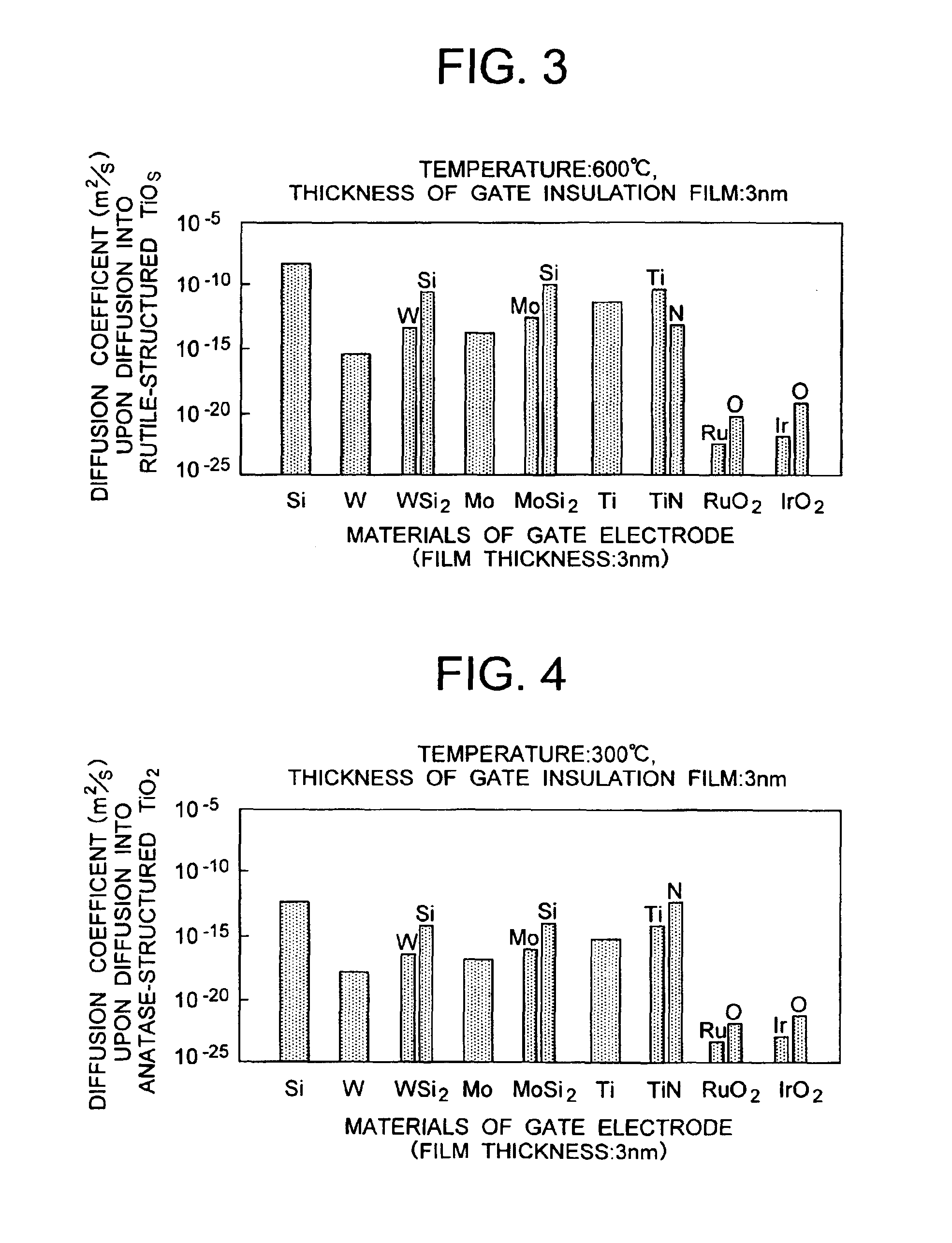
[0087]An insulation film 112 serves as a film for inter-element separation. The MOS transistor 102 of the memory cell is composed of a gate electrode film 105, a gate insulation film 106 and diffusion films 107 and 108. Reference numeral 104 denotes an element separation film. With a view to satisfying the requirement for miniaturization and high performance, titanium oxide is employed as a primary constituent material for forming the gate insulation film 106.

[0088]The gate insulation film 106 mentioned above is formed by resorting to, for example, a...

third embodiment

[0089]As the primary constituent material for the gate electrode film 105, ruthenium oxide or iridium oxide is used because then the diffusion of conductive elements into the gate insulation film 106 is difficult to occur upon heat treatment. This gate electrode film 105 may be implemented in a multi-layer structure having two or more layers as describe previously in conjunction with the invention.

[0090]The gate electrode film 105 can be formed by resorting to, for example, a chemical vapor deposition process, a sputtering process or the like. Further, an insulation film 109 of e.g. silicon oxide film is formed on the top and the side walls of the gate electrode film 105.

[0091]Connected to one diffusion film 107 of the memory cell selecting MOS transistor is a bit line 111 by way of a plug 110. Further formed over the whole top surface of the MOS transistor is an insulation film 112 which may be constituted, for example, by a BPSG (Boron-Doped Phosphor Silicate Glass) film, an SOG (...


PUM


Abstract

Gate insulation films each containing titanium oxide as a primary constituent material are formed on one major surface of a semiconductor substrate. Gate electrode films are formed in contact with the gate insulation films. The gate electrode films contain ruthenium oxide or alternatively iridium oxide as a primary constituent material. In order to prevent electrically conductive elements from diffusing into titanium oxide of the gate insulation films, ruthenium oxide or iridium oxide is effectively used as a primary constituent material of the gate electrodes. A semiconductor device can be realized in which occurrence of a leak current is suppressed by increasing a physical film thickness while sustaining desired dielectric characteristic.

Description

BACKGROUND OF THE INVENTION[0001]The present invention relates to a semiconductor device and a method of manufacturing the same.[0002]In recent years, in keeping with a trend of implementing the semiconductor device in a miniaturized structure, there has arisen the requirement that the gate of a transistor be realized in a length of 0.15 μm with the film thickness of the gate insulation film being decreased to less than 2 nm when silicon oxide (SiO2) is employed for the gate insulation film. In this conjunction, it is noted that such thickness of the gate insulation film as mentioned above will give rise to occurrence of a tunnel current of unignorable magnitude. To cope with this problem, it has been attempted to increase the physical film thickness while maintaining the desired dielectric characteristic by using an insulation material exhibiting higher dielectric constant (or permittivity) than SiO2.[0003]As a candidate for such high dielectric constant material, there may be ment...

Claims


Application Information

Patent Timeline
IPC IPC(8): H01L21/28H01L21/02H01L29/51H01L29/49H01L29/40H01L21/70H01L27/108H01L21/8242H01L21/316H01L29/43H01L21/8246H01L27/105H01L29/423H01L29/78
CPCH01L21/28088H01L21/28185H01L21/28194H01L29/4966H01L29/513H01L21/31604H01L27/10814H01L27/10873H01L27/10882H01L29/517H10B12/315H10B12/05H10B12/48H01L29/78
Inventor IWASAKI, TOMIOMIURA, HIDEOOHTA, HIROYUKIMORIYA, HIROSHI
Owner RENESAS ELECTRONICS CORP
Why Eureka
Try Eureka