[0010]As a first aspect of the invention, a method for manufacturing a
semiconductor device includes: partially forming an epitaxial growth stopper film on a
single crystal semiconductor substrate; sequentially depositing a first semiconductor layer and a second semiconductor layer on the semiconductor substrate by an epitaxial growth process, and forming a first groove penetrating through the second semiconductor layer and the first semiconductor layer on the semiconductor substrate, at a region inside from an outer
peripheral portion of the epitaxial growth stopper film, by partially etching the second semiconductor layer and the first semiconductor layer. The first aspect also includes forming a support body film on an entire surface of the semiconductor substrate, so as to fill the first groove and cover the second semiconductor layer, and a step of forming a support body in a shape covering the second semiconductor layer from the first groove to an element region, extending over the outer peripheral portion of the epitaxial growth stopper film, by partially etching the support body film. The first aspect further includes forming a second groove exposing a side surface of the first semiconductor layer, by sequentially etching the second semiconductor layer and the first semiconductor layer exposing from under the support body, forming a hollow portion between the semiconductor substrate and the second semiconductor layer, by selectively etching the first semiconductor layer interposing the second groove therebetween, under an etching condition that the first semiconductor layer is easier to etch than the second semiconductor layer, and forming an insulating layer in the hollow portion.
[0011]In the first aspect, the “epitaxial growth stopper film”, for example, is a film having an amorphous structure. When the first semiconductor layer and the second semiconductor layer are formed by the epitaxial growth process, a portion directly formed on the semiconductor substrate becomes a
single crystal structure, but a portion formed on the epitaxial growth stopper film becomes a polycrystalline structure or the amorphous structure, in the first semiconductor layer and the second semiconductor layer. In a case when the semiconductor substrate, for example, is a
single crystal silicon substrate, the first semiconductor layer, for example, is
silicon germanium (SiGe), and the second semiconductor layer, for example, is silicon (Si), a
silicon oxide (SiO2) film, for example, may be used as the epitaxial growth stopper film.
[0012]Also, the “element region” is a region where the SOI structure (in other words, a structure that a semiconductor layer exists on an insulating layer) is formed. To the semiconductor layer at an upper portion of the SOI structure (in other words, the second semiconductor layer), an element such as a transistor, for example, is formed.
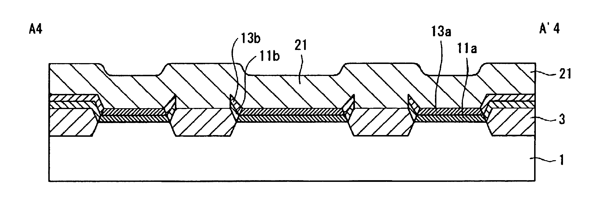
[0013]According to the first aspect, a portion which comes into contact with the support body (hereinafter, referred to as a “support body adjacent portion”) in the second semiconductor layer may be formed in the polycrystalline structure or the amorphous structure. Therefore, when the hollow portion is formed between the semiconductor substrate and the second semiconductor layer, not only the first semiconductor layer, but also the support body adjacent portion in the second semiconductor layer can be etched, thereby enabling to provide a space between the side surface of the second semiconductor layer and the support body. When the insulating layer is formed in the hollow portion, the stress of the second semiconductor layer can be relieved, as the side surface of the second semiconductor layer is separated from the support body. Therefore, desired transistor characteristics can be obtained.
[0014]As a second aspect of the invention, a method for manufacturing a semiconductor device includes sequentially depositing a first semiconductor layer and a second semiconductor layer on a single
crystal semiconductor substrate by an epitaxial growth process, forming a first groove penetrating through the second semiconductor layer and the first semiconductor layer on the semiconductor substrate, by partially etching the second semiconductor layer and the first semiconductor layer, and forming a support body film on an entire surface of the semiconductor substrate, so as to fill the first groove and cover the second semiconductor layer. The second aspect also includes forming a support body in a shape covering the second semiconductor layer from the first groove to an element region, by partially etching the support body film, and forming a second groove exposing a side surface of the first semiconductor layer, by sequentially etching the second semiconductor layer and the first semiconductor layer exposing from under the support body. The second aspect further includes a step of forming a hollow portion between the semiconductor substrate and the second semiconductor layer, by selectively etching the first semiconductor layer interposing the second groove therebetween, under an etching condition that the first semiconductor layer is easier to etch than the second semiconductor layer, forming an insulating layer in the hollow portion, and forming an epitaxial growth stopper film on the semiconductor substrate at a region sandwiched between a region forming the first groove and the element region before forming the first semiconductor layer, and the first semiconductor layer and the second semiconductor layer are also deposited on the epitaxial growth stopper film in the step of forming the first semiconductor layer and the second semiconductor layer.
