Deskewing method and apparatus, and data reception apparatus using the deskewing method and apparatus

a data reception and deskewing technology, applied in the field of semiconductor memory devices, can solve the problems of data skews and jitters, increasing manufacturing costs, and increasing manufacturing costs, and achieving the effect of increasing manufacturing costs, increasing manufacturing costs, and avoiding data skews

Inactive Publication Date: 2007-12-27
SAMSUNG ELECTRONICS CO LTD
View PDF2 Cites 63 Cited by
  • Summary
  • Abstract
  • Description
  • Claims
  • Application Information

AI Technical Summary

Problems solved by technology

As the speed of communications between semiconductor chips increases, skew and jitter in data transmitted between the semiconductor chips become more severe and problematic.
This method, however, imposes restrictions on the routing of signals, thereby increasing manufacturing costs.
Furthermore, even though PCB lines or signal lines are properly matched with one another, data skews are likely to occur due to inevitable factors such as manufacturing process, voltage, and temperature variations.
Due to such data skews, errors in the r

Method used


Image

  • Deskewing method and apparatus, and data reception apparatus using the deskewing method and apparatus
  • Deskewing method and apparatus, and data reception apparatus using the deskewing method and apparatus
  • Deskewing method and apparatus, and data reception apparatus using the deskewing method and apparatus

Examples


Embodiment Construction

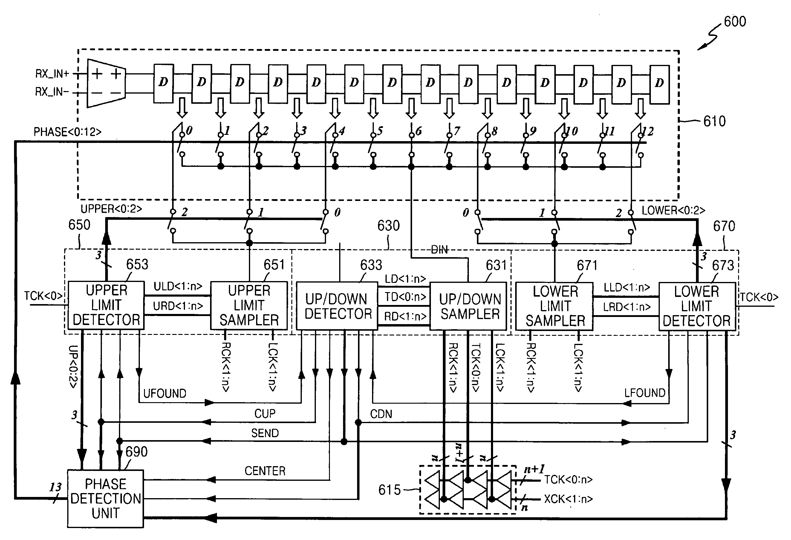
[0032]Exemplary embodiments of the present invention will now be described more fully with reference to the accompanying drawings. In the drawings, like reference numerals represent like elements.

[0033]Exemplary embodiments of the present invention will hereinafter be described in detail focusing more on receiving of a data signal having jitter and / or skew, however, exemplary embodiments of the present invention can also be applied to any data signal comprising jitters and / or skews.

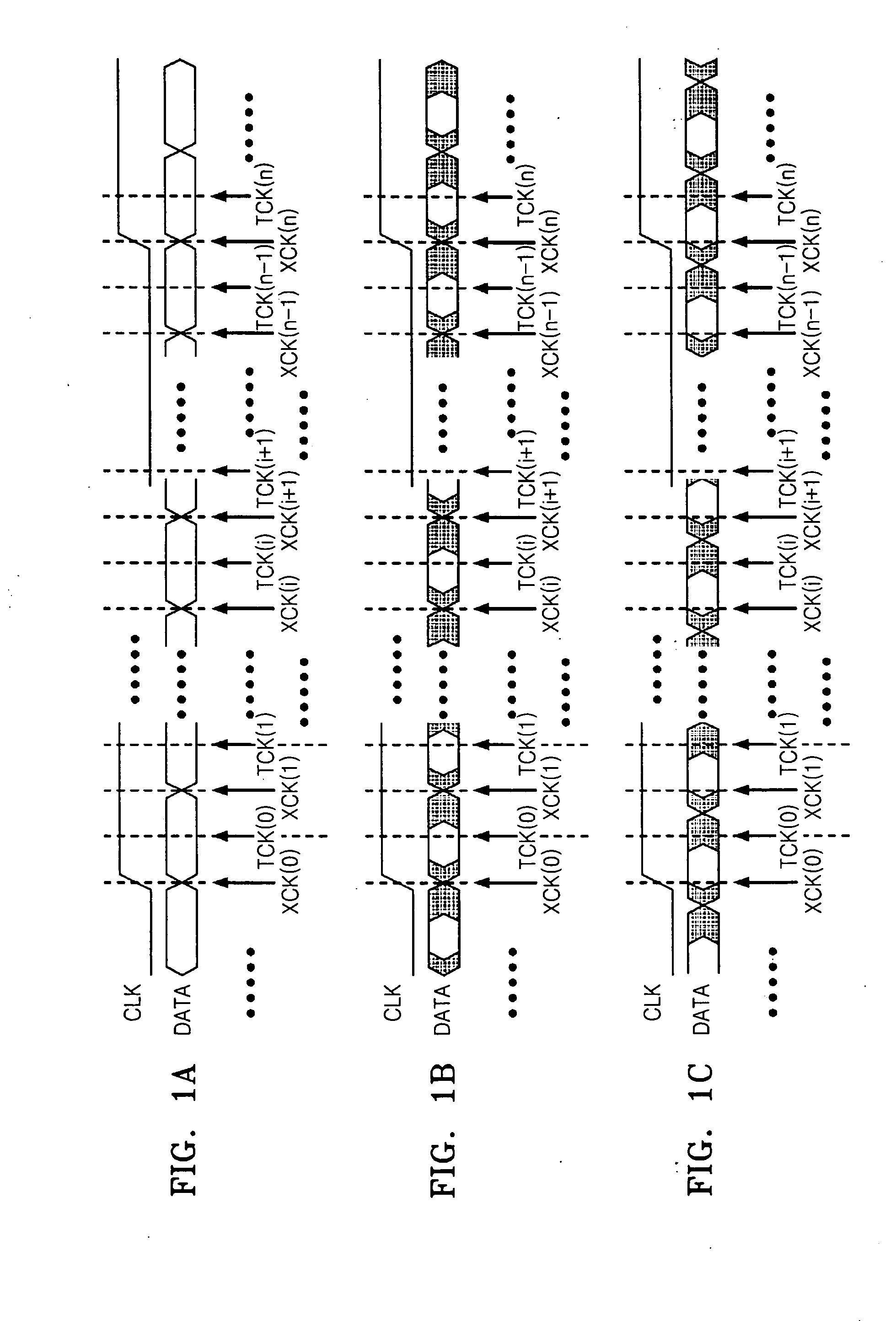
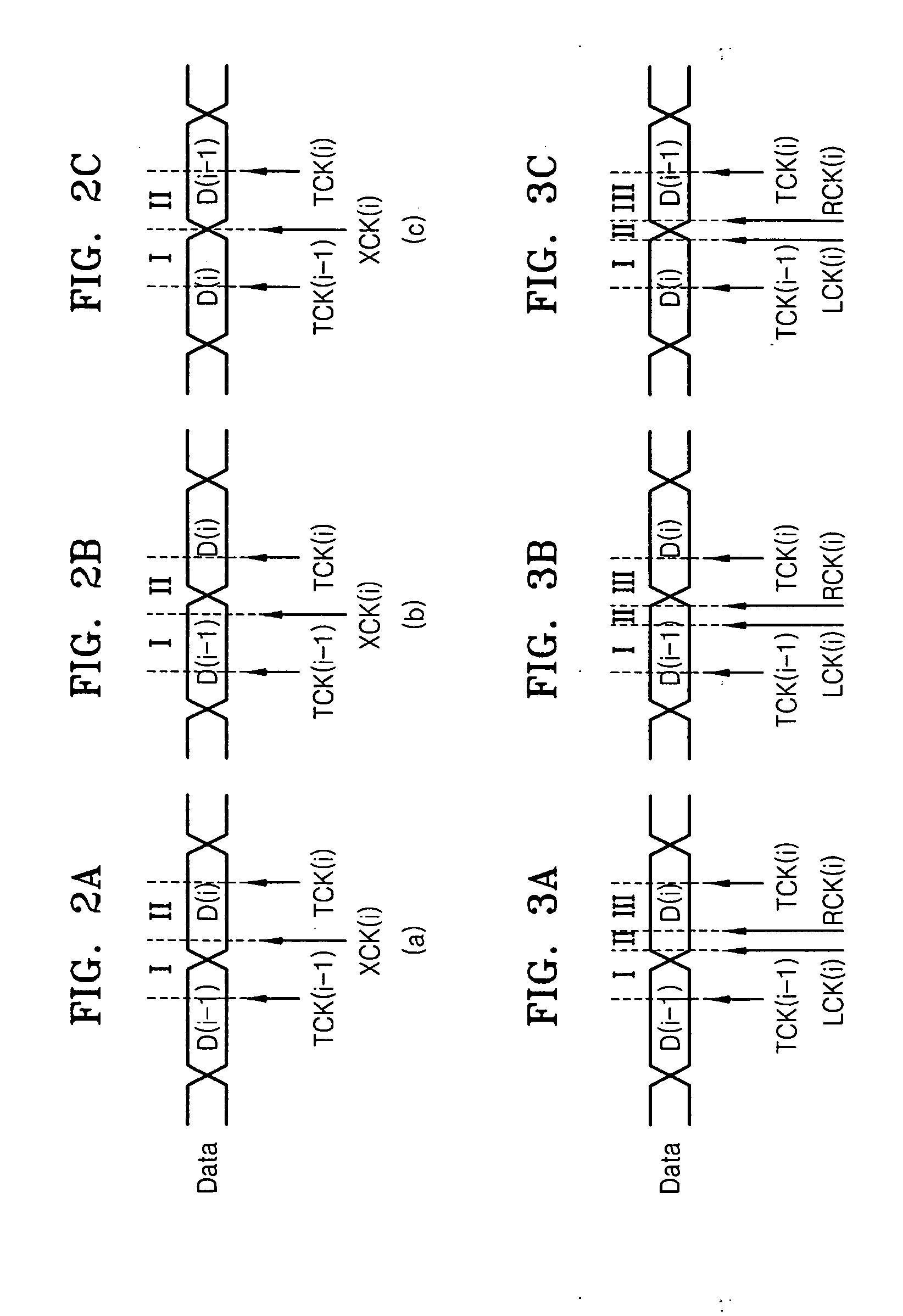
[0034]FIGS. 1A-1C are timing diagrams illustrating the relationship between a received data signal and a clock signal when transmitting data at a data rate of n. When transmitting data at a data rate of n, a total of n bits are transmitted during one cycle of a clock signal CLK. Referring to FIGS. 1A-1C, XCK represents an edge sampling clock signal, TCK represents a data sampling clock signal, and DATA represents a received data signal. The data signal DATA is sampled in response to the data sampling cloc...


PUM


Abstract

Deskewing method and apparatus, and a data reception apparatus using the deskewing method and apparatus, in which the deskewing apparatus includes an up/down detection unit, a lower limit detection unit, an upper limit detection unit, a phase detection unit, and a buffer unit. The up/down detection unit samples a received data signal in response to a data sampling clock signal, a first edge sampling clock signal, and a second edge sampling clock signal and determines in which of first through third areas of the data signal the logic level of the data signal transitions by using the result of the sampling, wherein the data sampling clock signal, the first edge sampling clock signal, and the second edge sampling clock signal are sequentially activated. The lower limit detection unit detects a lower limit of the first area if the logic level of the data signal transitions in the first area. The upper limit detection unit detects an upper limit of the third area if the logic level of the data signal transitions in the third area. The phase detection unit determines a delay amount indicating the amount by which the data signal is to be delayed according to the upper limit detected by the upper limit detection unit and the lower limit detected by the lower limit detection unit. The buffer unit delays the data signal by the delay amount determined by the phase detection unit. The deskewing apparatus can optimize data sampling by efficiently reducing data skew. In addition, the deskewing apparatus can minimize data restoration errors by reducing an accumulation of jitter.

Description

CROSS-REFERENCE TO RELATED PATENT APPLICATION[0001]This application claims the benefit of Korean Patent Application No. 10-2006-0058182, filed on Jun. 27, 2006, in the Korean Intellectual Property Office, the disclosure of which is incorporated herein in its entirety by reference.BACKGROUND OF THE INVENTION[0002]1. Technical Field[0003]The present disclosure relates to a semiconductor memory device, and more particularly, to a deskewing method and apparatus and a data reception apparatus using the deskewing method and apparatus in a semiconductor memory device.[0004]2. Discussion of the Related Art[0005]As the speed of communications between semiconductor chips increases, skew and jitter in data transmitted between the semiconductor chips become more severe and problematic. Accordingly, in order to restore desired data during communication between semiconductor chips, clock skew and clock jitter must be minimized for data transmitted between the semiconductor chips.[0006]To improve ...

Claims


Application Information

Patent Timeline
IPC IPC(8): H04L7/00
CPCH04L7/0337H04L7/033H03L7/091H04L7/00
Inventor CHOI, YOUNG-DON
Owner SAMSUNG ELECTRONICS CO LTD
Why Eureka
Try Eureka