Silicon-on-insulator (SOI) junction field effect transistor and method of manufacture

a junction field effect transistor and silicon-on-insulator technology, applied in the field of semiconductor devices, can solve the problem that in the last several decades little research has been done on jfet devices

Inactive Publication Date: 2008-01-03
DSM SOLUTIONS
View PDF5 Cites 46 Cited by
  • Summary
  • Abstract
  • Description
  • Claims
  • Application Information

AI Technical Summary

Problems solved by technology

However, because JFET devices are not typically used in today's semiconductor devic

Method used


Image

  • Silicon-on-insulator (SOI) junction field effect transistor and method of manufacture
  • Silicon-on-insulator (SOI) junction field effect transistor and method of manufacture
  • Silicon-on-insulator (SOI) junction field effect transistor and method of manufacture

Examples


Embodiment Construction

[0018]Various embodiments of the present invention will now be described in detail with reference to a number of drawings. The embodiments show a silicon-on-insulator (SOI) junction field effect transistor (JFET) and more particularly, complementary SOI JFETs, such as an SOI p-type JFET and SOI n-type JFET. Steps for manufacturing such devices are also described.

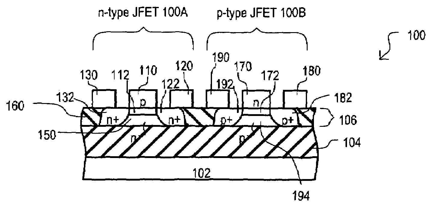
[0019]Referring now to FIG. 1, a cross-sectional diagram of a semiconductor device including complementary SOI JFET devices according to an embodiment is set forth and given the general reference character 100.

[0020]A semiconductor device 100 can include complementary JFETs (p-type and n-type) built on a SOI wafer. In the example shown, semiconductor device 200 includes a substrate 102, an insulating layer 104 and a device layer 106. Substrate 102 may be a silicon substrate, a quartz substrate, or other suitable material. Insulating layer 104 may be a silicon dioxide layer, or other suitable insulating layer. Device layer 10...


PUM


Abstract

A semiconductor device including complementary junction field effect transistors (JFETS) manufactured on a silicon on insulator (SOI) wafer is disclosed. A p-type JFET includes a control gate formed from n-type polysilicon and an n-type JFET includes a control gate formed from p-type polysilicon. The complementary JFETs may include four terminal JFETs having a back gate formed below a channel region. The back gate may be electrically connected to a control gate formed above a channel region via a cut region in an isolation structure. Furthermore, the complementary JFETs may be formed on strained silicon formed on a silicon germanium (SiGe) or silicon germanium carbon (SiGeC) layer, or the like.

Description

[0001]This application claims the benefit of U.S. Provisional Patent Application Ser. No. 60 / 799,787, filed May 11, 2006, U.S. patent application Ser. No. 11 / 261,873, filed Oct. 28, 2005, and U.S. patent application Ser. No. 11 / 452,442, filed Jun. 13, 2006, the contents all of which are incorporated by reference herein.TECHNICAL FIELD[0002]The present invention relates generally to semiconductor devices, and more particularly to semiconductor devices including a silicon-on-insulator (SOI) junction field effect transistor (JFET).BACKGROUND OF THE INVENTION[0003]Junction field effect transistors can have advantages over a metal-oxide-semiconductor field effect transistor (MOSFET) as device sizes decrease. One particular advantage includes the absence of a thin gate insulating layer as found in a typical. MOSFET. However, because JFET devices are not typically used in today's semiconductor devices, little research has been performed on JFET devices in the last several decades.[0004]One...

Claims


Application Information

Patent Timeline
IPC IPC(8): H01L29/80H01L29/00H01L31/112
CPCH01L21/26513H01L27/098H01L29/8086H01L29/66901H01L27/1203
Inventor KAPOOR, ASHOK KUMAR
Owner DSM SOLUTIONS
Why Eureka
Try Eureka