Optical modulator

Active Publication Date: 2008-01-03
SUMITOMO OSAKA CEMENT CO LTD
View PDF2 Cites 32 Cited by
  • Summary
  • Abstract
  • Description
  • Claims
  • Application Information

AI Technical Summary

Benefits of technology

[0041] According to the tenth aspect of the present invention, since the optical waveguide is the Mach-Zehnder type optical waveguide and the optical waveguide in the output side of the optical junction portion of the Mach-Zehnder type optical waveguide is configured by the two waveguides for radiation light with the output waveguide interposed therebetween, the radiation light generated at the optical junction portion is guided to the waveguide for radiation light and thus the propagation light which propagates in the output waveguide and the radiation light are efficiently separated from each other spatially.
[0042] According to the eleventh aspect of the present invention, since, in the optical junction portion, the two branch waveguides and the two waveguides for radiation light for configuring the Mach-Zehnder type optical waveguide are configured to be line symmetrical with respect to the light propagation direction of the output waveguide, the propagation light can be introduced into the output waveguide, and the radiation light can be introduced into the waveguide for radiation light. Furthermore, the propagation light can be suppressed from being introduced into the waveguide for radiation light, and the radiation light can be suppressed from being introduced into the output waveguide. Accordingly, it is possible to efficiently separate the propagation light and the radiation light from each other spatially.
[0043] According to the twelfth aspect of the present invention, since, in the optical junction portion, the width of each of the waveguides for radiation light is narrower than that of the output waveguide,

Problems solved by technology

Since Patent Document 4 is premised on lens coupling, there is a problem that the propagation light and the radiation light are mixed.
As a result, an extinction ratio of the optica

Method used


Image

  • Optical modulator
  • Optical modulator
  • Optical modulator

Examples


example 1

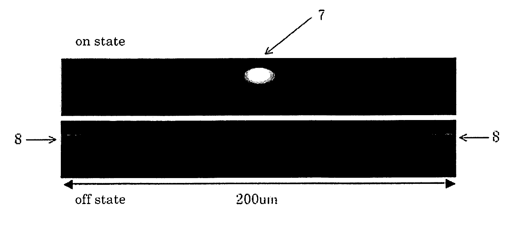
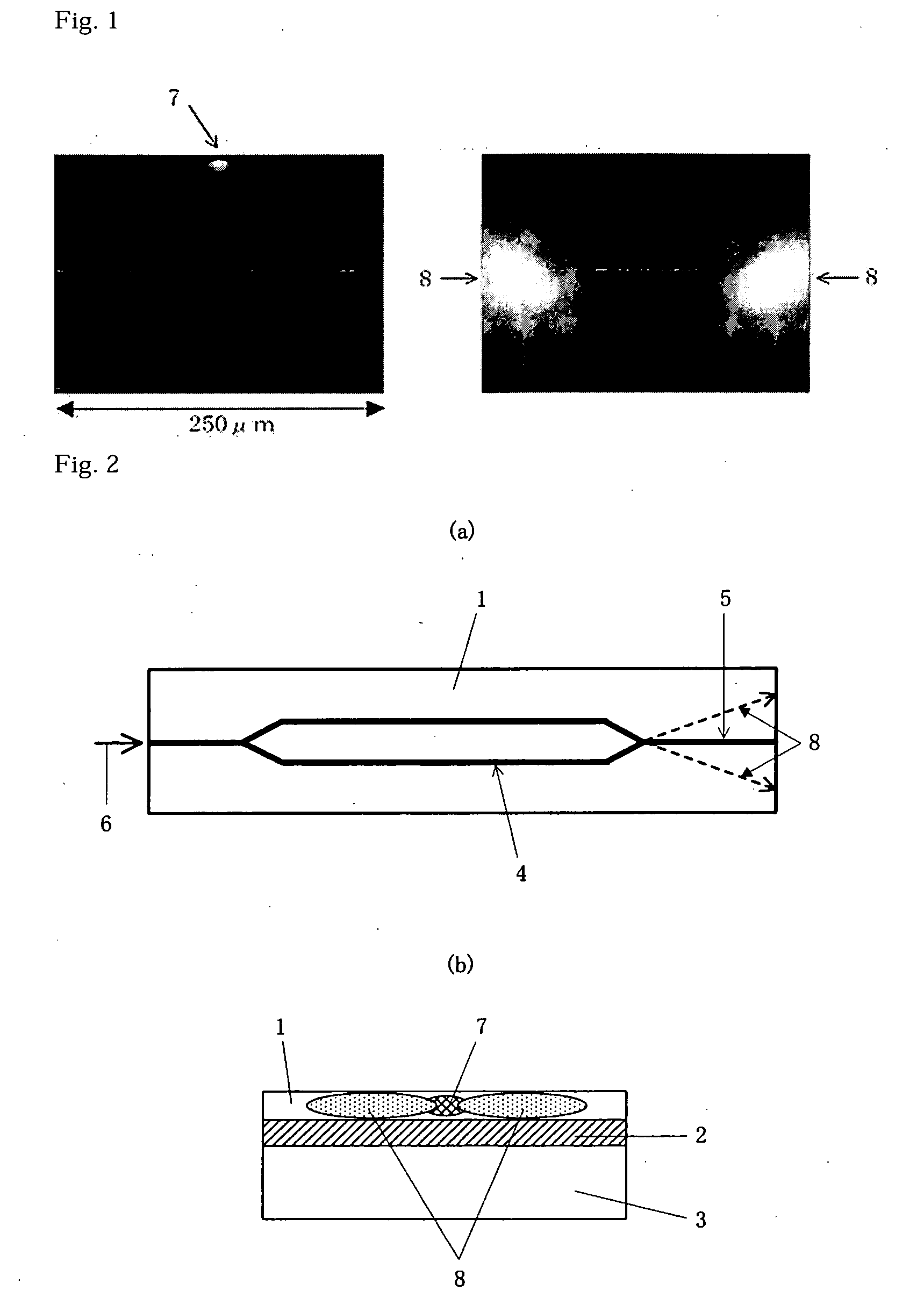
[0103] In an optical modulation element of a thin plate, an X-cut type LN substrate having a thickness of 500 μm was used as a substrate and an optical waveguide was formed in the top surface of the substrate by a Ti diffusing process. The optical waveguide is a Mach-Zehnder type optical waveguide as shown in FIG. 4 and the distance from an optical junction portion to the end portion of the substrate is 3500 μm. The bottom surface of the substrate was polished by a polishing machine until the thickness of the substrate becomes 10 μm, and was then attached to a reinforcement plate using an UV-curing adhesive as an adhesive layer. Next, a modulation electrode was formed by a plating process, a through-hole having a depth of 10 μm was formed in the way from the optical junction portion to the output end portion by a laser cutter as a shielding means and Al was attached to the concave portion. Thereafter, the substrate was cut to have a predetermined size, thereby manufacturing the thin...

example 2

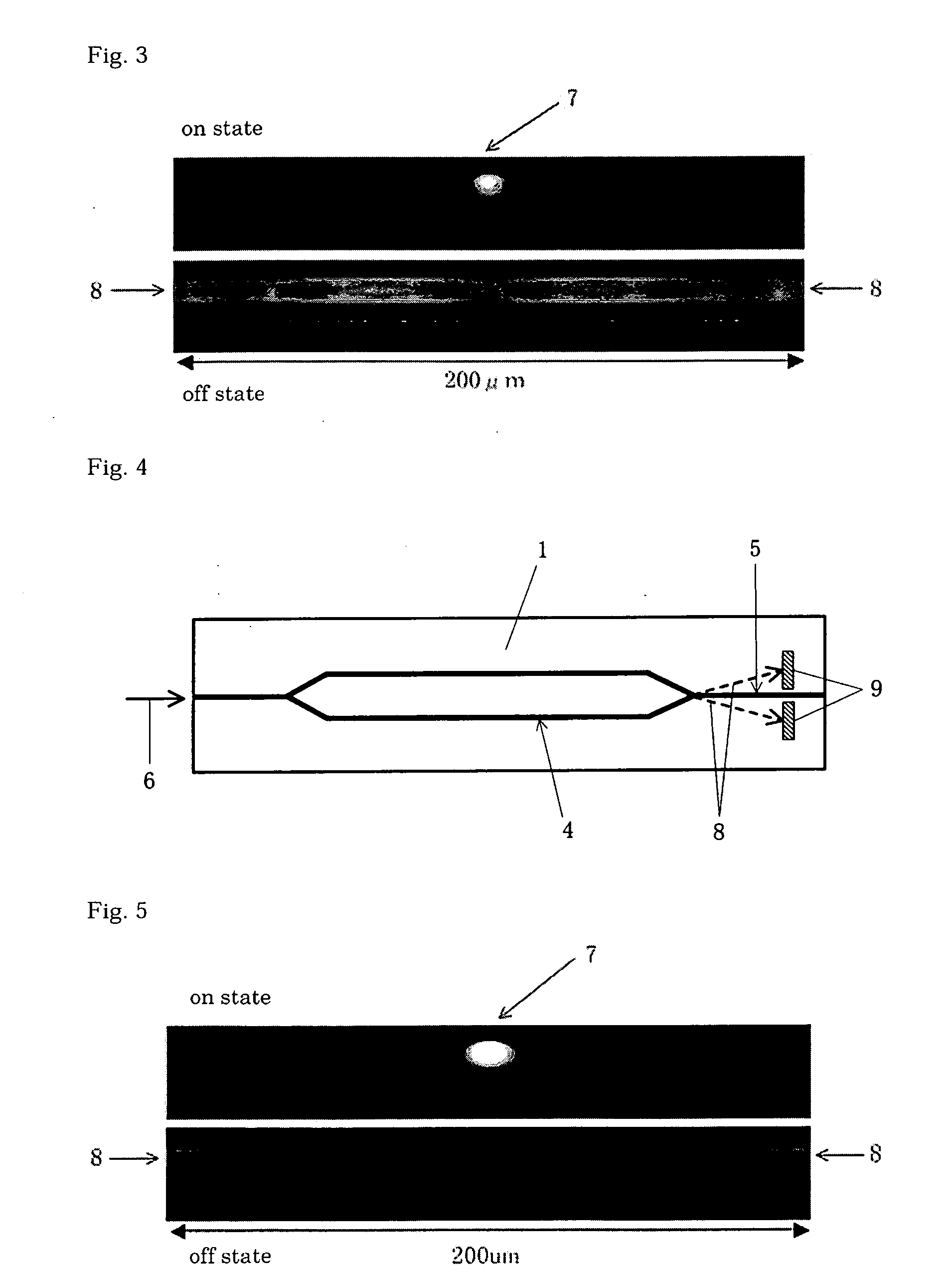
[0104] In an optical modulation element of a thin plate, an X-cut type LN substrate having a thickness of 500 μm was used as a substrate, an optical waveguide was formed in the top surface of the substrate by a Ti diffusing process, and high refractive index regions (Ti diffusion, a shortest distance from the central portion of the output waveguide to the high refractive index region: 15 μm) were formed in the both sides of the output waveguide. The optical waveguide is a Mach-Zehnder type optical waveguide as shown in FIG. 6 and the distance from an optical junction portion to the end portion of the substrate is 3500 μm. The bottom surface of the substrate was polished by a polishing machine until the thickness of the substrate becomes 10 μm, and was then attached to a reinforcement plate using an UV-curing adhesive as an adhesive layer. Next, a modulation electrode was formed by a plating process and the substrate was cut to have a predetermined size, thereby manufacturing the thi...

example 3

[0105] In an optical modulation element of a thin plate, an X-cut type LN substrate having a thickness of 500 μm was used as a substrate and an optical waveguide was formed in the top surface of the substrate by a Ti diffusing process. The optical waveguide is a Mach-Zehnder type optical waveguide as shown in FIG. 8 and the distance from an optical junction portion to the end portion of the substrate is 3500 μm. The bottom surface of the substrate was polished by a polishing machine until the thickness of the substrate becomes 10 μm, and was then attached to a reinforcement plate using an UV-curing adhesive as an adhesive layer. Light absorbing regions (material: Al, a shortest distance from the central portion of the output waveguide to the light absorbing region: 15 μm) were formed in the both sides of the output waveguide. Next, a modulation electrode was formed by a plating process and the substrate was cut to have a predetermined size, thereby manufacturing the thin plate havin...


PUM


Abstract

Provided is an optical modulator capable of efficiently separating radiation light and propagation light from each other or removing the radiation light in the optical modulator to suppress loss of the optical modulator and deterioration of an extinction ratio. In the optical modulator including a thin plate made of a material having an electrooptic effect and having a thickness of 20 μm or less; an optical waveguide formed in a top surface or a bottom surface of the thin plate; and a modulation electrode which is formed in the top surface of the thin plate to modulate light which propagates in the optical waveguide, the optical waveguide has an optical junction portion in which a plurality of optical waveguide portions are joined together and a shielding means for shielding a portion of radiation light radiated from the optical junction portion. The shielding means is a concave portion or a thorough-hole formed in the thin plate, a shortest distance from the waveguide to the shielding means is 5 to 10 μm, and the length of the shielding means in a direction perpendicular to the waveguide is at least 0.5 times the diameter of a fiber.

Description

BACKGROUND OF THE INVENTION [0001] 1. Field of the Invention [0002] The present invention relates to an optical modulator, and more particularly, to an optical modulator including a thin plate made of a material having an electrooptic effect and having a thickness of 20 μm or less. [0003] 2. Related Art Statement [0004] Conventionally, in an optical communication field or an optical measurement field, a waveguide type optical modulator in which an optical waveguide or a modulation electrode is formed on a substrate having an electrooptic effect is much used. [0005] Particularly, as multimedia has been developed, the amount of communication tends to increase and thus wider bandwidth of an optical modulation frequency needs to be realized. As a realizing means thereof, an external modulation method using a LN modulator or the like has been diversified. However, in order to realize the wider bandwidth of the LN modulator, velocity matching between a light wave and a microwave which is ...

Claims


Application Information

Patent Timeline
IPC IPC(8): G02F1/035
CPCG02B2006/12145G02F2001/212G02F1/035G02B2006/12147G02F1/212
Inventor KONDOU, KATSUTOSHIICHIOKA, MASAYUKISHINRIKI, TAKASHISUGAMATA, TOHRUICHIKAWA, JUNICHIRO
Owner SUMITOMO OSAKA CEMENT CO LTD
Why Eureka
Try Eureka