Fast lithography compliance check for place and route optimization

a compliance check and optimization technology, applied in the field of layout design, can solve the problems of slow and laborious manual fixing of hot spots, increasing difficulty in achieving reasonable fidelity (including resolution and depth of focus), and slow use of orcs to detect hot spots

Active Publication Date: 2008-01-03
SYNOPSYS INC
View PDF34 Cites 50 Cited by
  • Summary
  • Abstract
  • Description
  • Claims
  • Application Information

AI Technical Summary

Benefits of technology

[0014]Other embodiments perform image simulation and evaluation as just described, i.e. locally, and also repeat the image simulation and evaluation at a global level on the layout resulting from application of the correction rules, followed by place and route, or tapeout if no defects remain. Still other embodiments do not perform image simulation and evaluation locally between application of detection and correction rules and instead perform image simulation and evaluation only at a global level on a layout generated by place and route, and a set of regions identified by such global operations are then used with above-described detection rules (which are applied locally to each identified region in the set) to identify a subset of regions that can be corrected by application of correction rules. The subset of regions to be corrected is typically, but not necessarily, smaller than the set of regions identified by the global operations

Problems solved by technology

Accordingly it has become increasingly difficult to achieve reasonable fidelity (including resolution and depth of focus) between (a) a layout as designed in a computer and (b) shapes of circuit elements formed in a wafer after fabrication, which normally involves a number of processes such as photolithography followed by metal deposition and chemical mechanical polishing.
Manual fixing of hot spots is slow and laborious.

Method used


Image

  • Fast lithography compliance check for place and route optimization
  • Fast lithography compliance check for place and route optimization
  • Fast lithography compliance check for place and route optimization

Examples


Embodiment Construction

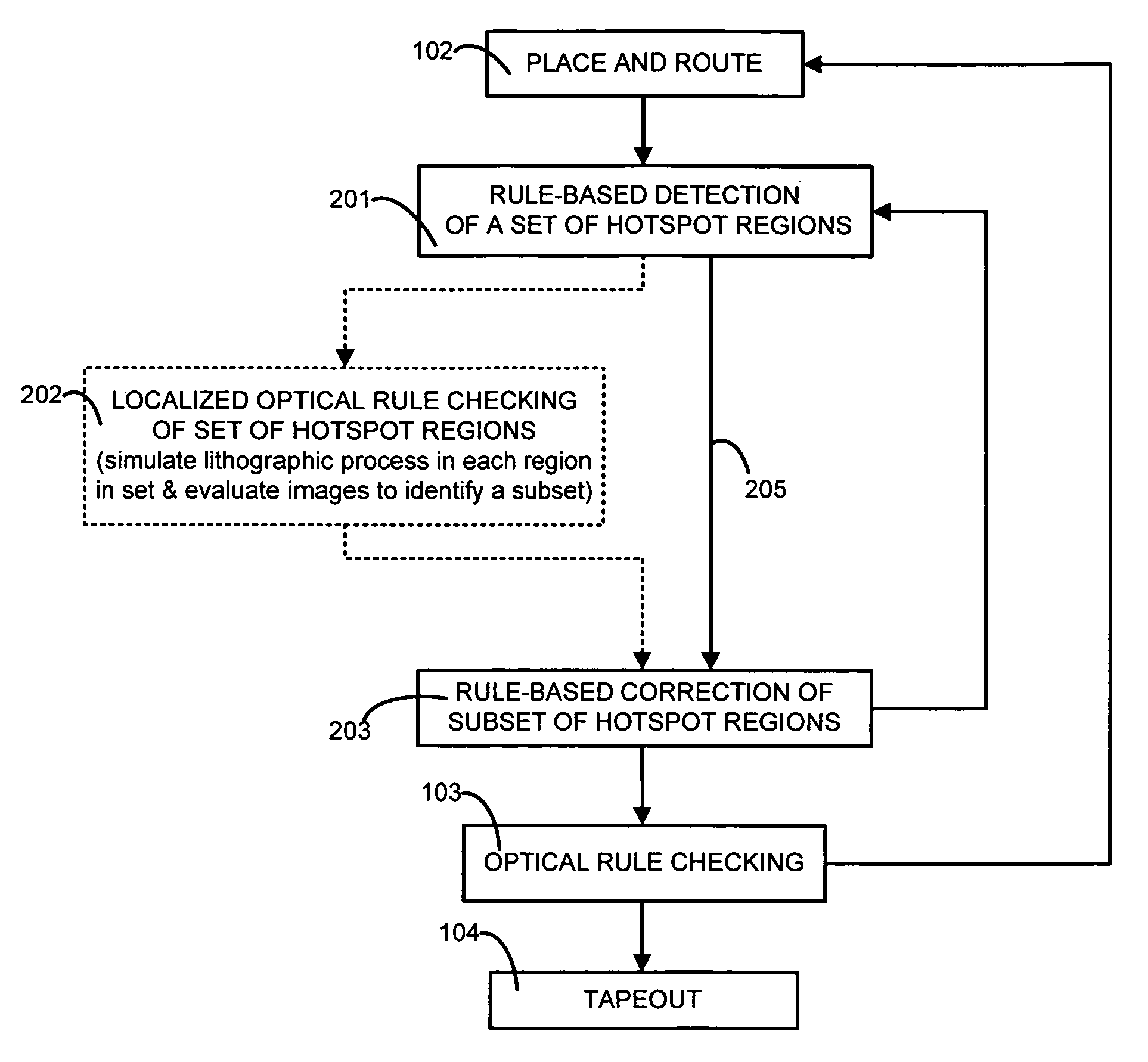
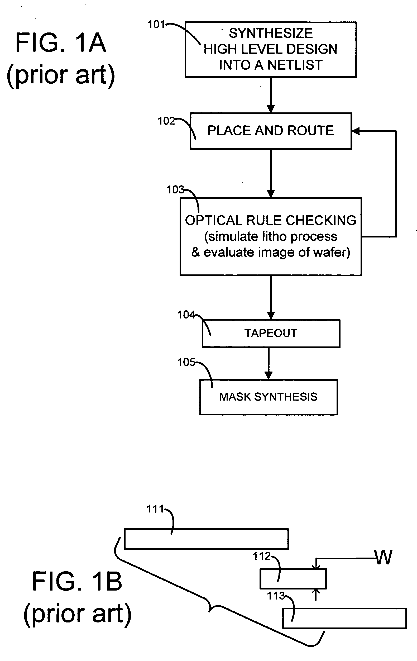
[0030]A computer 150 (FIG. 10A) is programmed, in accordance with the invention, to perform acts 201 and 203 (FIG. 2A) in any order relative to a place-and-route operation 102 and an ORC operation 103.

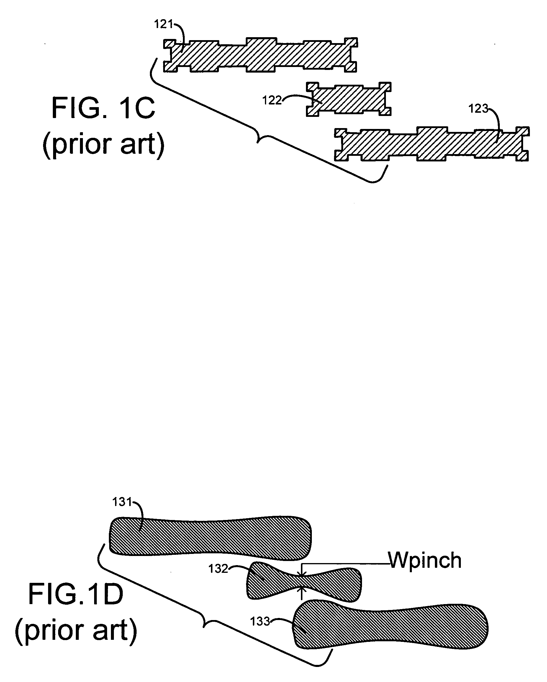
[0031]Operation 102 is performed using any prior art place-and-route tool, such as the Astro product available from Synopsys, Inc. Moreover, in prior art ORC operation 103, a simulation is performed of a lithographic process to be used to build the integrated circuits in a semiconductor wafer, and the simulation generates image intensities to which are applied one or more evaluation criteria such as measurement of critical dimension of contours. Each contour in a simulated image represents a side or a corner of a polygon in the layout input to the simulation.

[0032]In some embodiments of the invention, computer 150 is programmed to perform prior art ORC operation 103 as follows: (1) Simulate wafer image intensities at a given defocus condition, (2) Use a threshold on the wafer image int...


PUM


Abstract

A computer is programmed to use at least one rule to identify from within a layout of an IC design, a set of regions likely to fail if fabricated unchanged. An example of such a rule of detection is to check for presence of two neighbors neither of which fully overlaps a short wire or an end of a long wire. The computer uses at least another rule to change at least one region in the set of regions, to obtain a second layout which is less likely to fail in the identified regions. An example of such a rule of correction is to elongate at least one of the two neighbors. The computer may perform optical rule checking (ORC) in any order relative to application of the rules, e.g. ORC can be performed between detection rules and correction rules i.e. performed individually on each identified region prior to correction.

Description

BACKGROUND[0001]1. Field of the Invention[0002]The invention relates to design of layouts used in fabrication of semiconductor wafers. More specifically, the invention relates to a method and an apparatus for rule-based detection of pinches, bridges and similar hot spot regions in wires of an integrated circuit (IC) chip and repair of the regions.[0003]2. Related Art[0004]In the manufacture of integrated circuit (IC) chips, minimum feature sizes have been shrinking according to Moore's law. Currently the minimum feature size is smaller than the wavelength of light used in the optical imaging system. Accordingly it has become increasingly difficult to achieve reasonable fidelity (including resolution and depth of focus) between (a) a layout as designed in a computer and (b) shapes of circuit elements formed in a wafer after fabrication, which normally involves a number of processes such as photolithography followed by metal deposition and chemical mechanical polishing.[0005]One prior...

Claims


Application Information

Patent Timeline
IPC IPC(8): G06F17/50
CPCG03F7/70433G06F17/5081G03F7/705G06F30/398
Inventor MILOSLAVSKY, ALEXANDERLUKPAT, GERARD
Owner SYNOPSYS INC
Why Eureka
Try Eureka