Logic compatible storage device

a logic and storage device technology, applied in the field of semiconductor devices, can solve the problems of specific process steps in the standard cmos-based logic process, create complications, and not only increase the wafer cost, but also fall short of the peak performance that the most advanced standard logic process can deliver. achieve the effect of improving the reliability of the memory cell, reducing leakage current for the memory array, and saving the chip area

Inactive Publication Date: 2008-01-10
TAIWAN SEMICON MFG CO LTD
View PDF8 Cites 36 Cited by
  • Summary
  • Abstract
  • Description
  • Claims
  • Application Information

AI Technical Summary

Benefits of technology

[0011]By forming a capacitor in metallization layers, chip area is saved. Further, the transistor isolates the non-volatile memory cell from other memory cells in the same memory array,...

Problems solved by technology

Integrating “non-volatile memory”-specific process steps into the standard CMOS-based logic process creates complications.
This prior approach not only typically increases the wafer cost, but it also falls short of the peak performance that the most advanced standard logic process can deliver.
Also, due to the cycling-induced degradation of the SiO2, the previous technique of subjecting all of the non-volatile memory cell components to higher...

Method used


Image

  • Logic compatible storage device
  • Logic compatible storage device
  • Logic compatible storage device

Examples


Embodiment Construction

[0018]The making and using of the presently preferred embodiments are discussed in detail below. It should be appreciated, however, that the present invention provides many applicable inventive concepts that can be embodied in a wide variety of specific contexts. The specific embodiments discussed are merely illustrative of specific ways to make and use the invention, and do not limit the scope of the invention.

[0019]A novel non-volatile memory cell and a method of forming the same are provided. The operations of the preferred embodiments are discussed. Throughout the various views and illustrative embodiments of the present invention, like reference numbers are used to designate like elements.

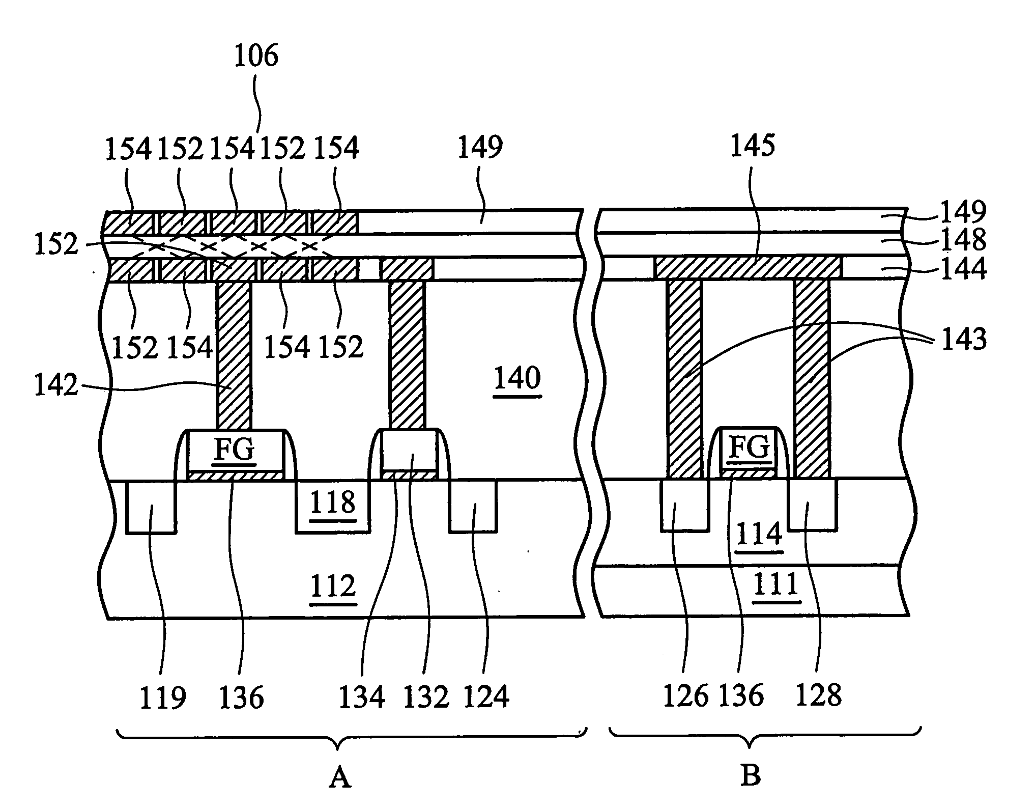
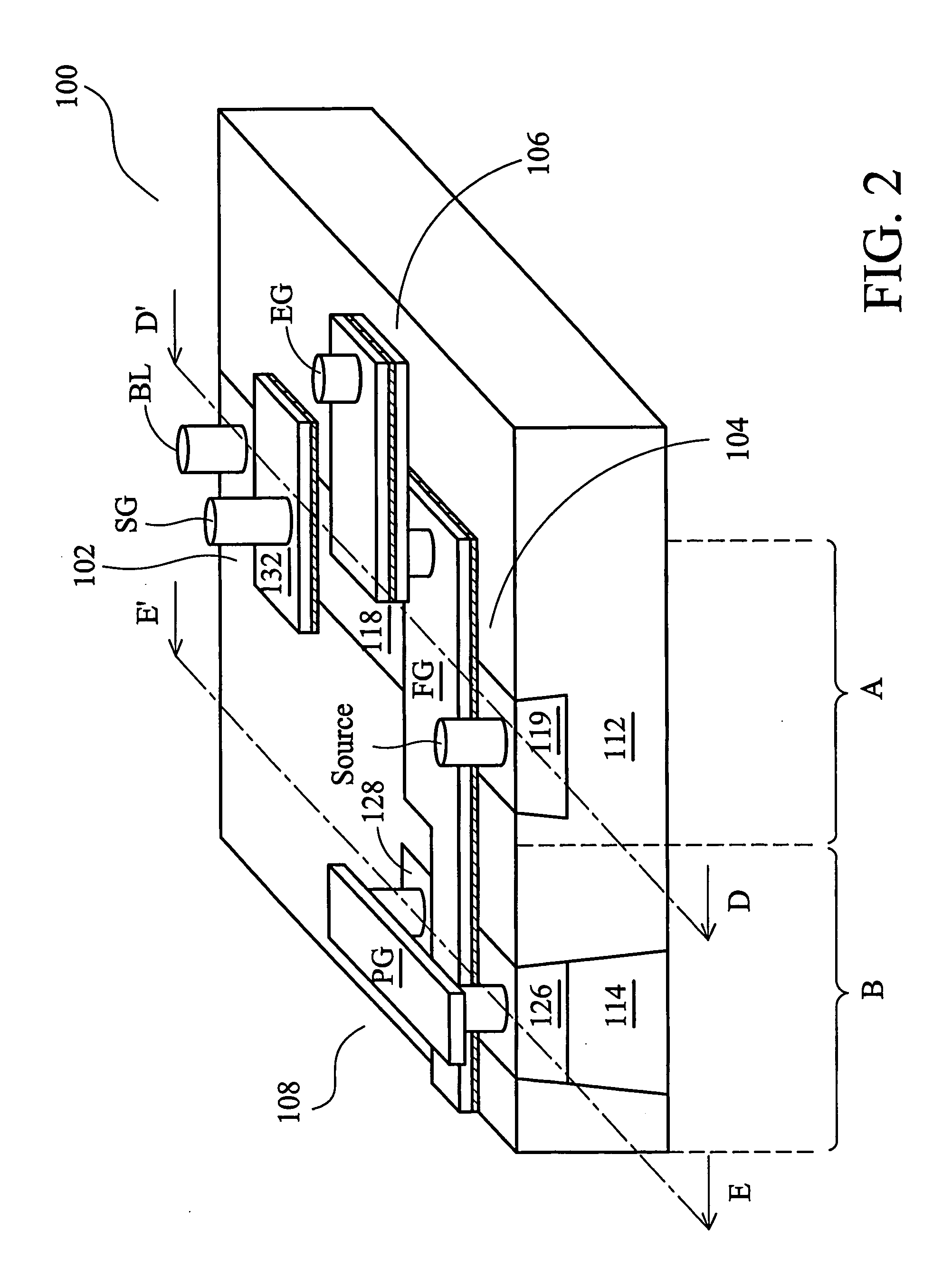
[0020]FIG. 2 illustrates a perspective view of a non-volatile memory cell 100, which comprises a transistor 102, a first capacitor (also referred to as an erase-tunneling capacitor) 104, a second capacitor (also referred to as a coupling capacitor) 106, and a third capacitor (also referred to ...


PUM


Abstract

A non-volatile memory cell and a method of manufacturing the same are provided. The non-volatile memory cell includes a floating gate over a semiconductor substrate, a first capacitor comprising a first plate, the floating gate, and a dielectric therebetween, a second capacitor comprising a second plate, the floating gate, and a dielectric therebetween, a third capacitor comprising a third plate connected to the floating gate, and a fourth plate, wherein the third and fourth plates are formed in metallization layers over the semiconductor substrate. The first plate of the first capacitor includes a first doped region and a second doped region in the semiconductor substrate. The non-volatile memory cell further includes a transistor comprising a gate electrode over the semiconductor substrate, wherein a source/drain region of the transistor is connected to the first doped region of the first capacitor.

Description

TECHNICAL FIELD[0001]This invention relates generally to semiconductor devices, and more particularly to memory cells, and even more particularly to the structure and manufacturing methods of non-volatile memory cells.BACKGROUND[0002]A non-volatile memory cell retains information stored in the memory cell even when the power is turned off. To create a non-volatile memory cell, typically a standard CMOS-based logic process is used as a starting foundation. Next, additional process steps are incorporated into the logic process flow to create the non-volatile memory cell. Examples of such additional process steps include second polysilicon deposition, junction dopant optimization, etc. Integrating “non-volatile memory”-specific process steps into the standard CMOS-based logic process creates complications. Consequently, embedded non-volatile memory technologies generally lag behind advanced logic fabrication processes by several generations. For a system-on-chip (SOC) approach, which r...

Claims


Application Information

Patent Timeline
IPC IPC(8): H01L29/76
CPCG11C16/0433H01L27/11558H01L27/11521H01L27/115H10B41/60H10B69/00H10B41/30
Inventor HSU, TE-HSUNLIN, YUNG-TAOLIN, DEREKYEH, JACK
Owner TAIWAN SEMICON MFG CO LTD
Why Eureka
Try Eureka