Positioning method, processing system, measurement method of substrate loading repeatability, position measurement method, exposure method, substrate processing apparatus, measurement method, and measurement apparatus

a technology of substrate loading repeatability and processing system, which is applied in the direction of photomechanical equipment, instruments, optics, etc., can solve the problems of reducing yield, reducing the accuracy of search alignment marks, and inconvenient circuit properties, so as to improve the processing efficiency of mark measurement, the effect of repeatability of substrate loading

Inactive Publication Date: 2008-01-17
NIKON CORP
View PDF4 Cites 135 Cited by
  • Summary
  • Abstract
  • Description
  • Claims
  • Application Information

AI Technical Summary

Benefits of technology

[0023] In this manner, outer shape variation of the object caused by A. offset, B. pre-alignment and repeatability of the wafer loading to the processing apparatus in the previous layer processing apparatus, and variation in a mark position due to a difference of the outer shape reference coordinate system are measured beforehand, and based on the measurement results, mark measurement can be adjusted. With this adjustment, when the mark position on the object loaded into the processing apparatus is measured using the mark measurement unit, the mark can always be located within the measurement field of the mark measurement unit, and the mark positions can be measured without fail. As a consequence, the processing with high accuracy and high throughput can be achieved based on measurement results of the mark positions.
[0025] With this apparatus, before the object is loaded into the processing apparatus, the pre-measurement apparatus measures the position coordinates in the outer shape reference coordinate system of the marks on the object, and based on the measurement results, the adjustment unit adjust the position of the measurement field of the mark measurement unit, and therefore the marks can be contained within the measurement field without fail.
[0027] With this method, since the loading repeatability is measured using results of the measurement of position information of the mark formed on the substrate (the substrate on which a device pattern is to be transferred) that is normally performed during substrate processing (e.g. exposure processing), it is unnecessary not only to use an exclusive datum wafer as in the related art, but also to suspend the processing. Accordingly, the substrate loading repeatability can be measured without reducing processing efficiency.
[0028] According to a fourth aspect of the present invention, there is provided a position measurement method in which position information that indicates a position of a substrate whose position is set to a predetermined datum position is measured, the method comprising: a process in which loading repeatability of the substrate disposed at the datum position is measured using the measurement method of substrate loading repeatability of the present invention; and a process in which the position of the substrate is adjusted in accordance with tendency of the loading repeatability, and position information of a mark formed on the substrate is measured. In such a case, since the substrate loading repeatability can be measured using the measurement method of substrate loading repeatability of the present invention, processing efficiency of the mark measurement improves.
[0029] According to a fifth aspect of the present invention, there is provided an exposure method in which a predetermined pattern is transferred onto a substrate, the method comprising: a substrate measurement process in which position information that indicates a position of the substrate is obtained using the position measurement method of the present invention; and a transfer process in which position control of the substrate is performed based on the position information of the substrate obtained in the substrate measurement process, and the pattern is transferred onto the substrate while performing. In such a case, since the transfer is performed while performing position control of the substrate using the position information of the substrate obtained using the position measurement method of the present invention, exposure with high throughput and high accuracy can be achieved.

Problems solved by technology

However, an inconvenience may occur in the properties of the circuit if the overlay accuracy between the layers is poor.
In such a case, the chip does not satisfy desired properties, and in the worst case, the chip becomes defective, which reduces the yield.
In such a case, the items referred to below become, for example, causes of errors of the positions of search alignment marks.
However, sometimes an outer shape of a wafer slightly deviates due to warpage of the wafer or the like, which deviates the positions of search marks with respect to each wafer at times, even when the outer shape of the wafer is detected and the wafer is loaded based on the outer shape as a datum.
Also, sometimes wafer loading repeatability is decreased due to insufficient adjustment of a mechanism that loads the wafer into an exposure apparatus on wafer loading, changes with time or the like.
However, also from the viewpoint of throughput, it is not preferable to suspend the process in order to measure loading repeatability using such a datum wafer.
Moreover, in the case measurement of the wafer loading repeatability is performed only at the time of the maintenance, the occurrence of abnormality in the wafer loading repeatability cannot be recognized until the measurement is performed, which may reduce the yield until the measurement is performed.

Method used


Image

  • Positioning method, processing system, measurement method of substrate loading repeatability, position measurement method, exposure method, substrate processing apparatus, measurement method, and measurement apparatus
  • Positioning method, processing system, measurement method of substrate loading repeatability, position measurement method, exposure method, substrate processing apparatus, measurement method, and measurement apparatus
  • Positioning method, processing system, measurement method of substrate loading repeatability, position measurement method, exposure method, substrate processing apparatus, measurement method, and measurement apparatus

Examples


Embodiment Construction

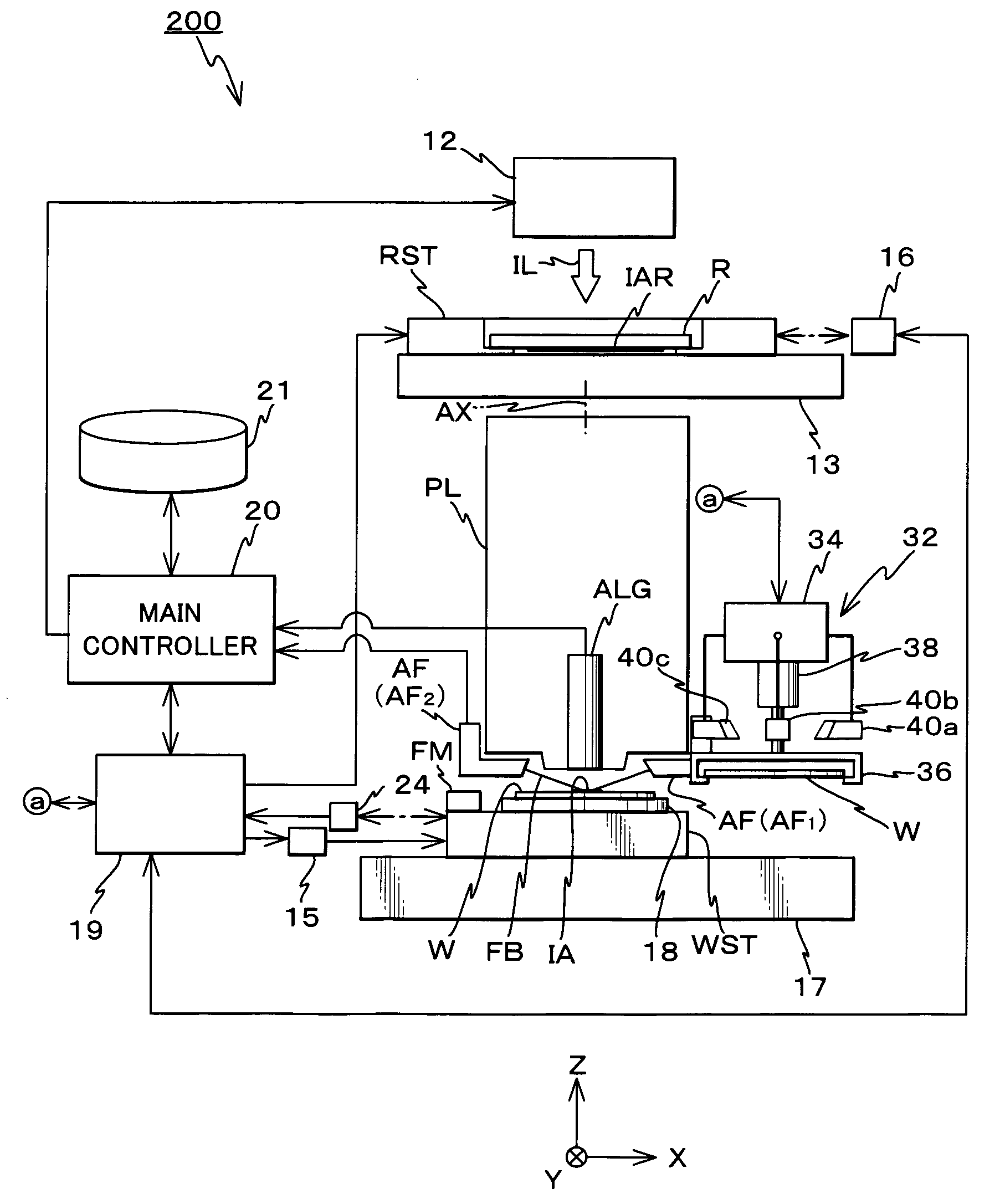
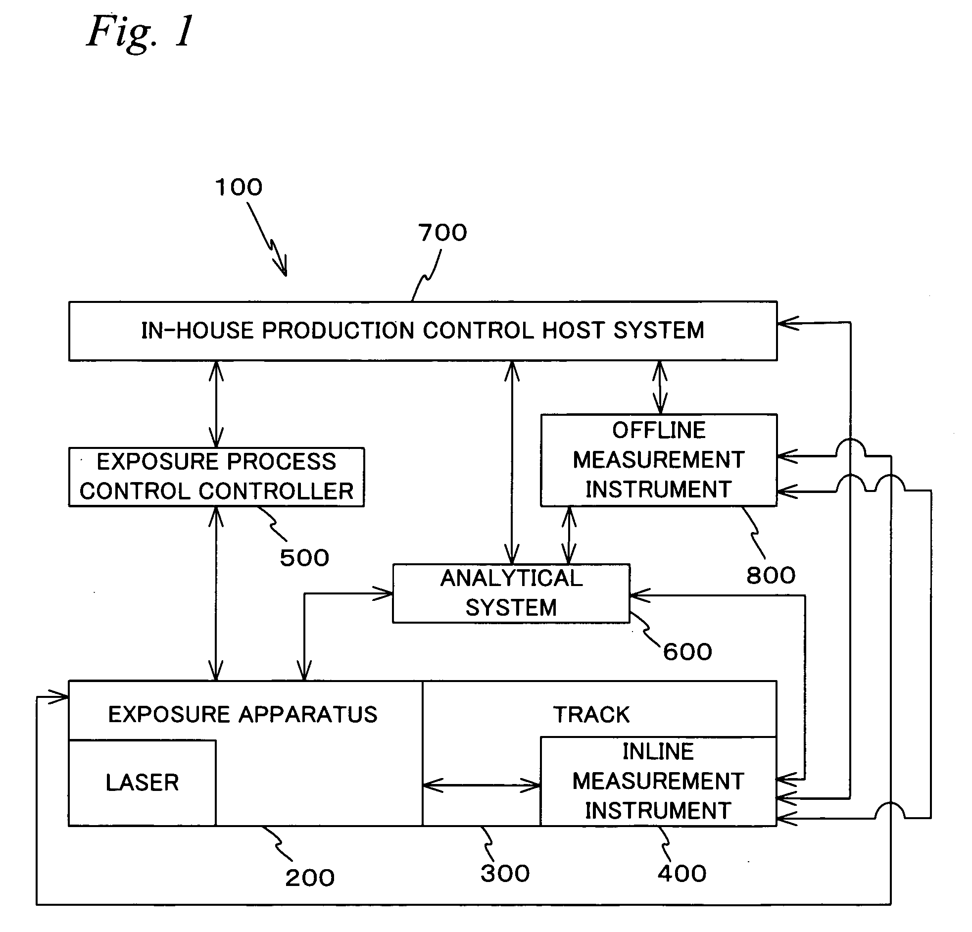
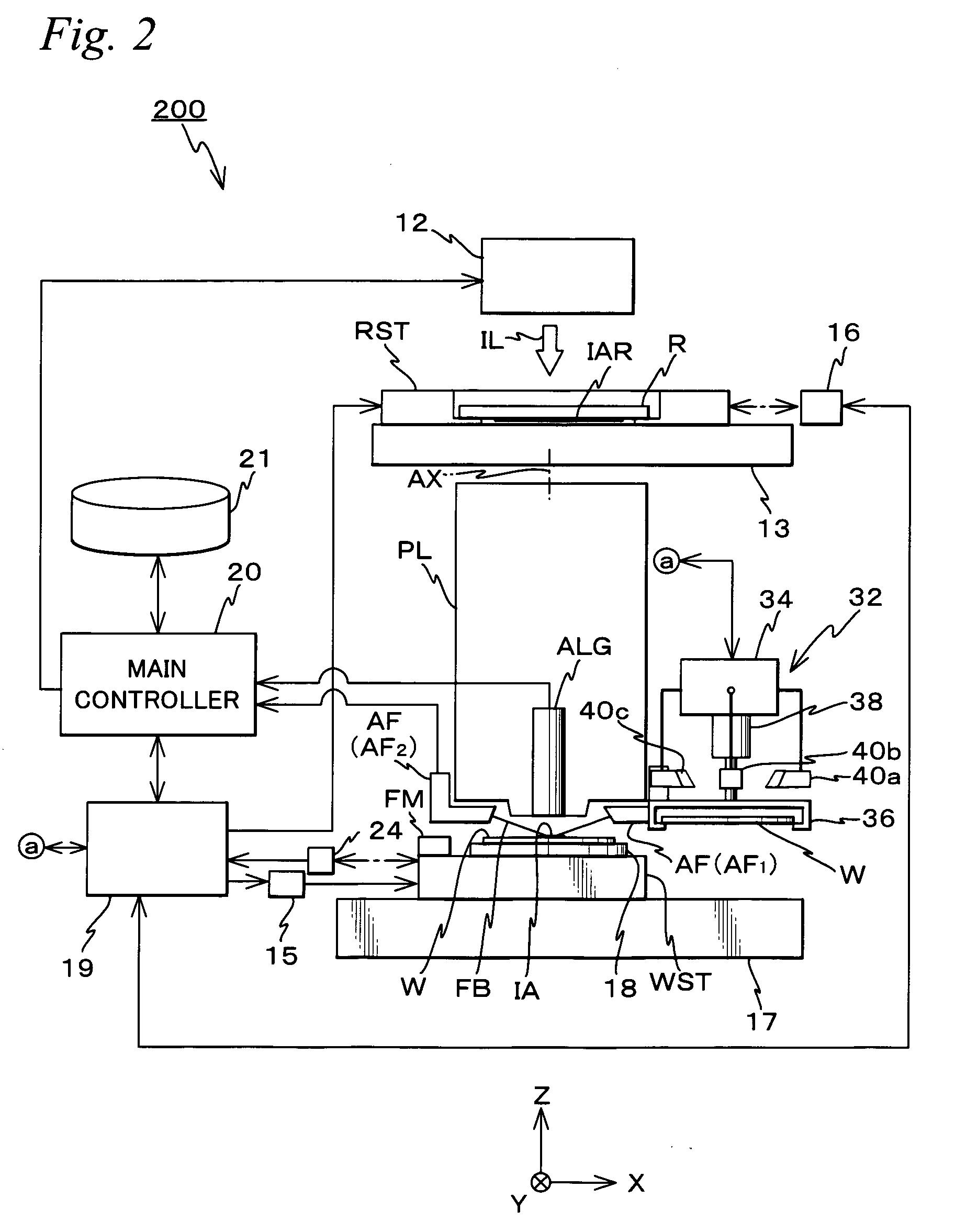
[0085] An embodiment of the present invention will be described below, referring to FIGS. 1 to 19. FIG. 1 schematically shows the entire configuration of a processing system 100 of the embodiment, in which a positioning method related to the present invention is carried out.

[0086] Processing system 100 is located in a ‘substrate processing factory’ where devices such as microdevices are manufactured by processing a substrate (hereinafter generally referred to as a ‘wafer W’) such as a semiconductor wafer or glass plate as an object. As is shown in FIG. 1, processing system 100 is equipped with an exposure apparatus 200 that comprises a light source such as laser light source, and a coating / developing apparatus (hereinafter referred to as a ‘track’) 300 that is disposed adjacent to exposure apparatus 200. Within track 300, an inline measurement instrument 400 is arranged.

[0087] The combination of exposure apparatus 200 and track 300 can be regarded as a substrate processing apparat...


PUM


Abstract

An edge of a surface to be measured of wafer and each of search alignment marks on the wafer are detected by an inline measurement instrument or the like that operates independently of an exposure apparatus, and position coordinates of the search marks in an X′Y′ coordinate system, which is a two-dimensional coordinate system substantially parallel to the surface to be measured and is set by a position of a notch of the wafer, are measured. Then, in pre-alignment performed when loading the wafer into the exposure apparatus, the edge of the wafer is detected, and from the detection results, position information of the object in the X′Y′ coordinate system is measured. Further, a relative position in the X′Y′ coordinate system of the wafer to be loaded into the exposure apparatus based on measurement results of the pre-alignment with respect to a measurement field of an alignment system that measures positions of the search marks on the wafer is adjusted based on measurement results of the inline measurement instrument or the like.

Description

CROSS-REFERENCE TO RELATED APPLICATIONS [0001] This application is a continuation of International Application No. PCT / JP2005 / 015764, with an international filing date of Aug. 30, 2005, the disclosure of which is hereby incorporated herein by reference in its entirety, which was not published in English. This non-provisional application also claims the benefit of Provisional Application No. 60 / 716,920 filed Sep. 15, 2005, the disclosure of which is hereby incorporated herein by reference in its entirety.BACKGROUND OF THE INVENTION [0002] 1. Field of the Invention [0003] The present invention relates to positioning methods, processing systems, measurement methods of substrate loading repeatability, position measurement methods, exposure methods, substrate processing apparatuses, measurement methods, and measurement apparatuses, and more particularly, for example, in a photolithography process for manufacturing semiconductor devices, liquid crystal display devices, imaging devices, th...

Claims


Application Information

Patent Timeline
Patent Type & Authority Applications(United States)
IPC IPC(8): G01B11/00
CPCG03F9/7011H01L21/682H01L21/681G03F9/7019G03F7/70775G03F9/7088
Inventor ISHII, YUUKIOKITA, SHINICHI
Owner NIKON CORP
Why Eureka
Try Eureka