Demodulation circuit, ic, and communication device

a demodulation circuit and communication device technology, applied in the field of demodulation circuits, ic and communication devices, can solve the problems of large size, large amount, and large electric current consumption of led

Inactive Publication Date: 2008-01-17
SHARP KK
View PDF4 Cites 11 Cited by
  • Summary
  • Abstract
  • Description
  • Claims
  • Application Information

AI Technical Summary

Benefits of technology

[0021]The present invention was made in view of the foregoing problems. An object of the present invention is to provide a demodulation circuit, an IC, and a communication device, each easily capable of selecting and demodulating a signal whose jitter component is small out of a plurality of supplied signals.

Problems solved by technology

However, in order to obtain a light output of 100 mW / sr specified in IrDA standard, an LED consumes an electric current of approximately 400 mA or more.
Consequently, an LED consumes an electric current of 1.6A or more, which is a very large amount.
Consequently, the communication device must have a structure against the heat, resulting in a larger size.
When a smaller device is required in the case of mobile phones, a communication device in a larger size is against the original intention.
As described above, it is difficult to increase transmission light intensity of a communication device, and therefore it is necessary to increase reception sensitivity of the communication device.
Normally, applying a large bias voltage leads to cost up of a whole system.
However, in a case of a lens of large diameter, light flux incident to the lens from all directions is required to be converged on the photodiode or the phototransistor, which makes an optical design very troublesome.
However, Document 1 has a problem as follows: in a case of a sufficiently slow optical signal, demodulation of the electric signal subjected to the logical disjunction can be carried out without any problem.
The electric signal having the jitter is subjected to the logical disjunction, resulting in an electric signal having so large jitter that a signal processing circuit cannot process the jitter.
Consequently, demodulation of the electric signal becomes difficult.
This results in communication loss.
Consequently, a pulse width or a pulse position of the preambles change regardless of light intensity, and accordingly it is impossible to judge whether the change is due to light intensity or not.
Consequently, it is uncertain whether pulses can be supplied sufficiently for PLL synchronization.
However, this causes reduction of an effective band of communications and requires all transmitters to be designed to be capable of lengthening a preamble.

Method used


Image

  • Demodulation circuit, ic, and communication device
  • Demodulation circuit, ic, and communication device
  • Demodulation circuit, ic, and communication device

Examples


embodiment 1

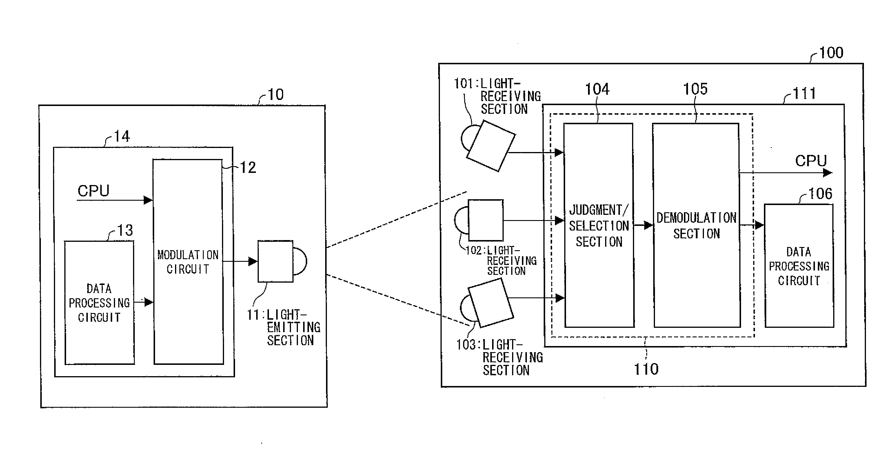
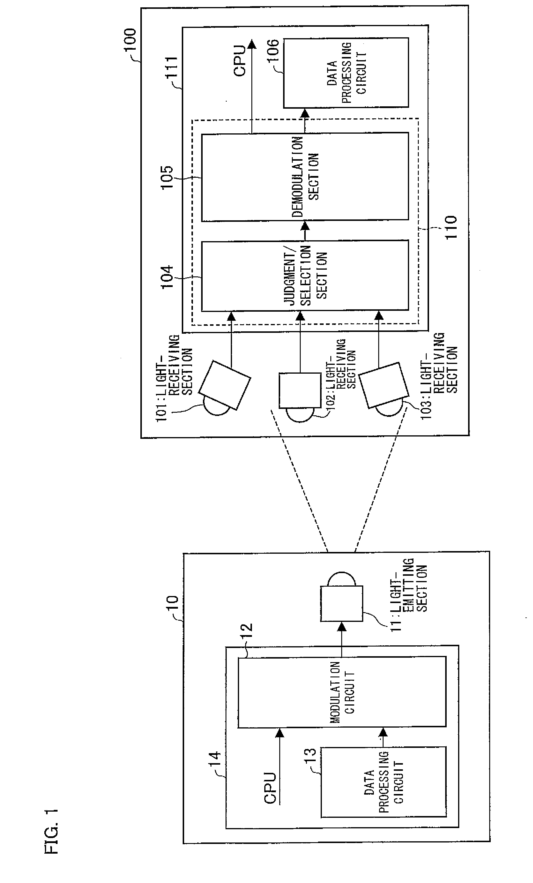
[0045]The following explains an embodiment of the present invention with reference to FIGS. 1 to 7. FIG. 1 is a block diagram showing communications between a transmitter 10 and a receiver 100 including light-receiving sections 101 to 103. The transmitter 10 and the receiver 100 include user interfaces such as a display section and an operation section, CPUs, and memories which are irrelevant to the subject matters of the present invention and therefore are omitted in the drawings.

[0046]The transmitter 10 and the receiver 100 in the following explanation include an optical communication function. A general communication method using an infrared ray (e.g. IrDA) is used in the present embodiment. However, the present invention is not limited to this. The present invention is applicable to optical communication methods for visible light communications using light other than an infrared ray, and to wireless communication methods using radio waves having high directivity.

[0047]With refer...

embodiment 2

[0166]With reference to FIGS. 8 to 12, the following explains another embodiment of the present invention. Note that, structures other than those explained in the present embodiment are the same as those in Embodiment 1. For convenience of explanation, members having the same functions as those illustrated in drawings of Embodiment 1 are given the same reference numerals and explanations thereof will be omitted here.

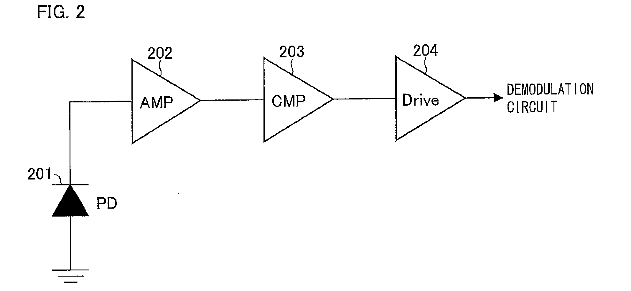
[0167]In Embodiment 1, an explanation was made as to a case where the light-receiving section 101 receives very weak light as illustrated in FIG. 1. In the present embodiment, it is assumed that the light-receiving section 101 does not receive an optical signal at all. At that time, as no signal is supplied, the gain of the amplifier 202 of the light-receiving section 101 is at the maximum.

[0168]Consequently, there is a case that even a little disturbing noise (such as an electric noise from a device, a variation in power source voltage, and a little change in disturbing...


PUM


Abstract

The demodulation circuit of the present invention is a demodulation circuit, connected with a plurality of light-receiving sections each for receiving an optical signal and converting the signal into a binary pulse signal, operable to select and demodulate a pulse signal out of pulse signals that are supplied from the light-receiving sections, respectively, the demodulation circuit including: a judgment and selection section for detecting timing with which High level and Low level of each of the pulse signals are switched and for selecting at least one pulse signal based on the timing; and a demodulation section for demodulating the pulse signal selected by the judgment and selection section. Consequently, the demodulation circuit easily selects and demodulates a signal whose jitter component is small out of a plurality of supplied signals.

Description

[0001]This non-provisional application claims priority under 35 U.S.C. §119(a) on Patent Application No. 2006-194902 filed in Japan on Jul. 14, 2006, the entire contents of which are hereby incorporated by reference.FIELD OF THE INVENTION[0002]The present invention relates to: a demodulation circuit for demodulating a reception signal; and an IC and a communication device including the demodulation circuit.BACKGROUND OF THE INVENTION[0003]Recently, many devices include infrared communication functions. Infrared communications use light and therefore have high directivity. Accordingly, communications are possible only when light transmitted from a light-emitting section of a communication device at least has light intensity which allows a light-receiving section of another communication device to receive the light in a surveyable range without any obstacles. For that reason, a communication distance and a light-receiving angle of the light communication depend on transmission light i...

Claims


Application Information

Patent Timeline
Patent Type & Authority Applications(United States)
IPC IPC(8): H03K5/125H04B10/10H04B10/105H04B10/22H04B10/07H04B10/11H04B10/116H04B10/516H04B10/524H04B10/58H04B10/61H04L25/08
CPCH03K5/1252H04L7/04H04B10/1141H04B10/1121
Inventor NAOE, HITOSHIFUKAE, FUMIHIROSAKAI, KOJIOHSAWA, SHOHEI
Owner SHARP KK
Why Eureka
Try Eureka