Supercharge Your Innovation With Domain-Expert AI Agents!

Process integration scheme of SONOS technology

Active Publication Date: 2008-01-17
CHARTERED SEMICONDUCTOR MANUFACTURING
View PDF15 Cites 0 Cited by
  • Summary
  • Abstract
  • Description
  • Claims
  • Application Information

AI Technical Summary

Benefits of technology

"The present invention provides a structure and method of manufacturing a memory device with improved performance and reliability. The method involves forming a charge storing film and a pad layer on a substrate, followed by the formation of isolation trenches and regions. A gate layer is then formed over the substrate, and the charge storing film and pad layer are removed in non-cell regions. The technical effects of this invention include improved programming precision, reduced programmable error, and improved reliability of the memory device."

Problems solved by technology

For instance, some of these advantages may be mutually contradictory, in that they cannot be simultaneously present in a single embodiment.

Method used


Image

  • Process integration scheme of SONOS technology
  • Process integration scheme of SONOS technology
  • Process integration scheme of SONOS technology

Examples


first example embodiment

I. First Example Embodiment

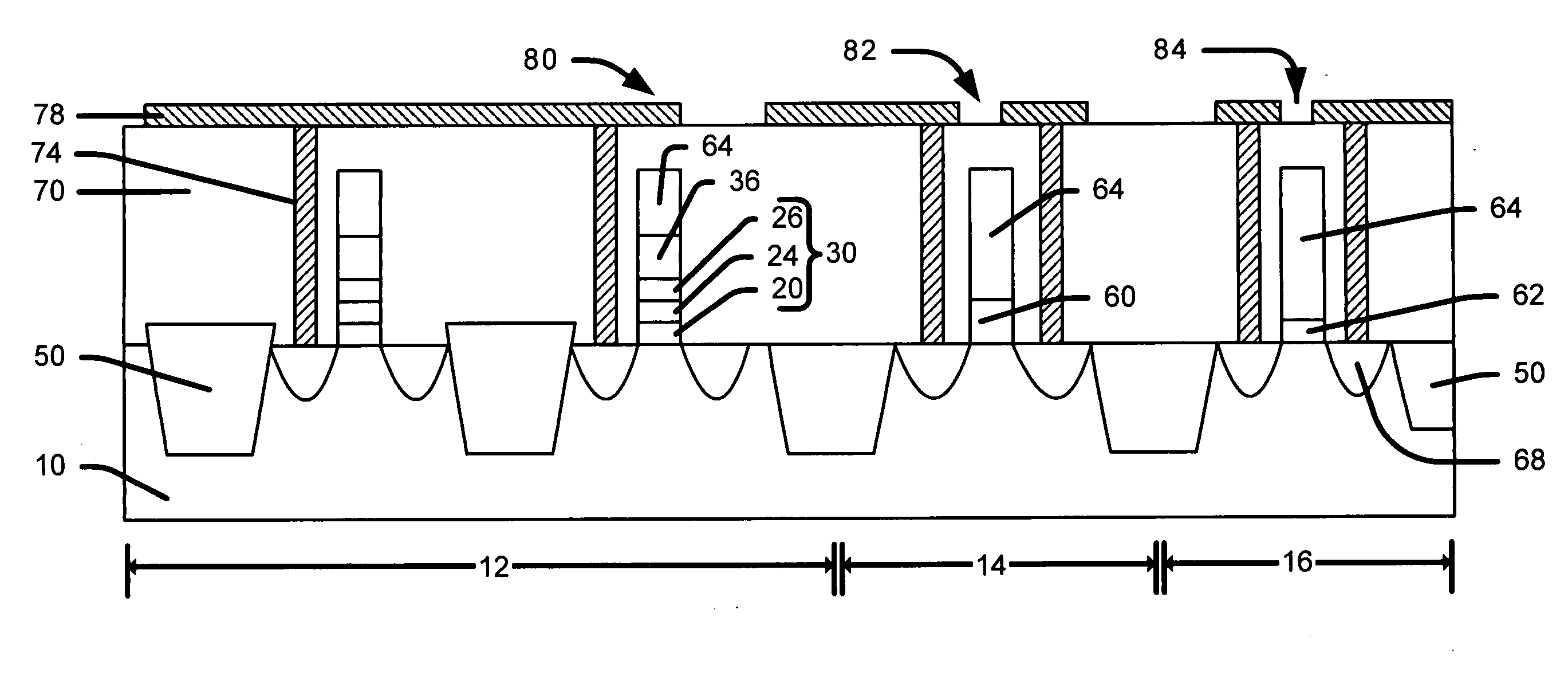
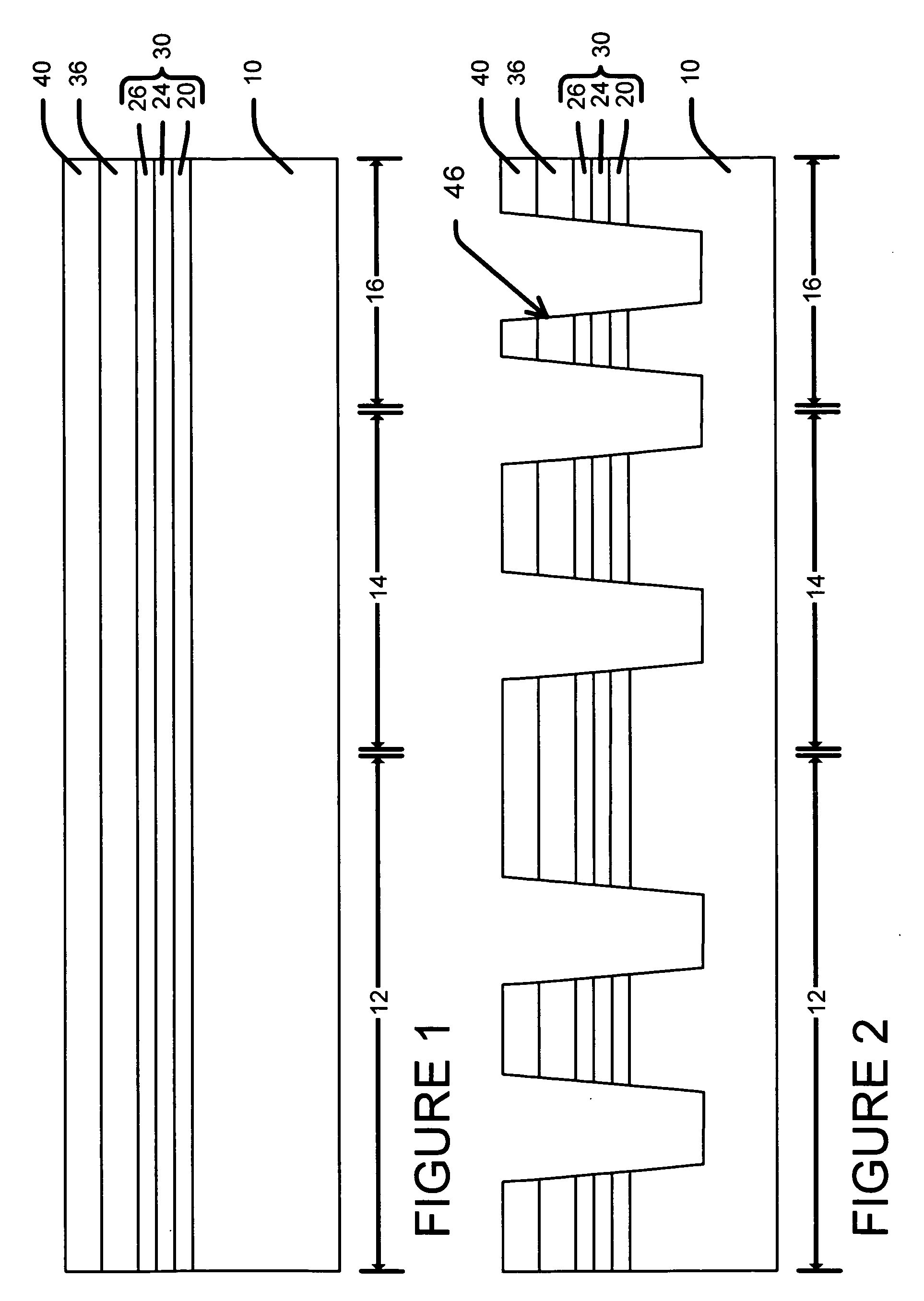
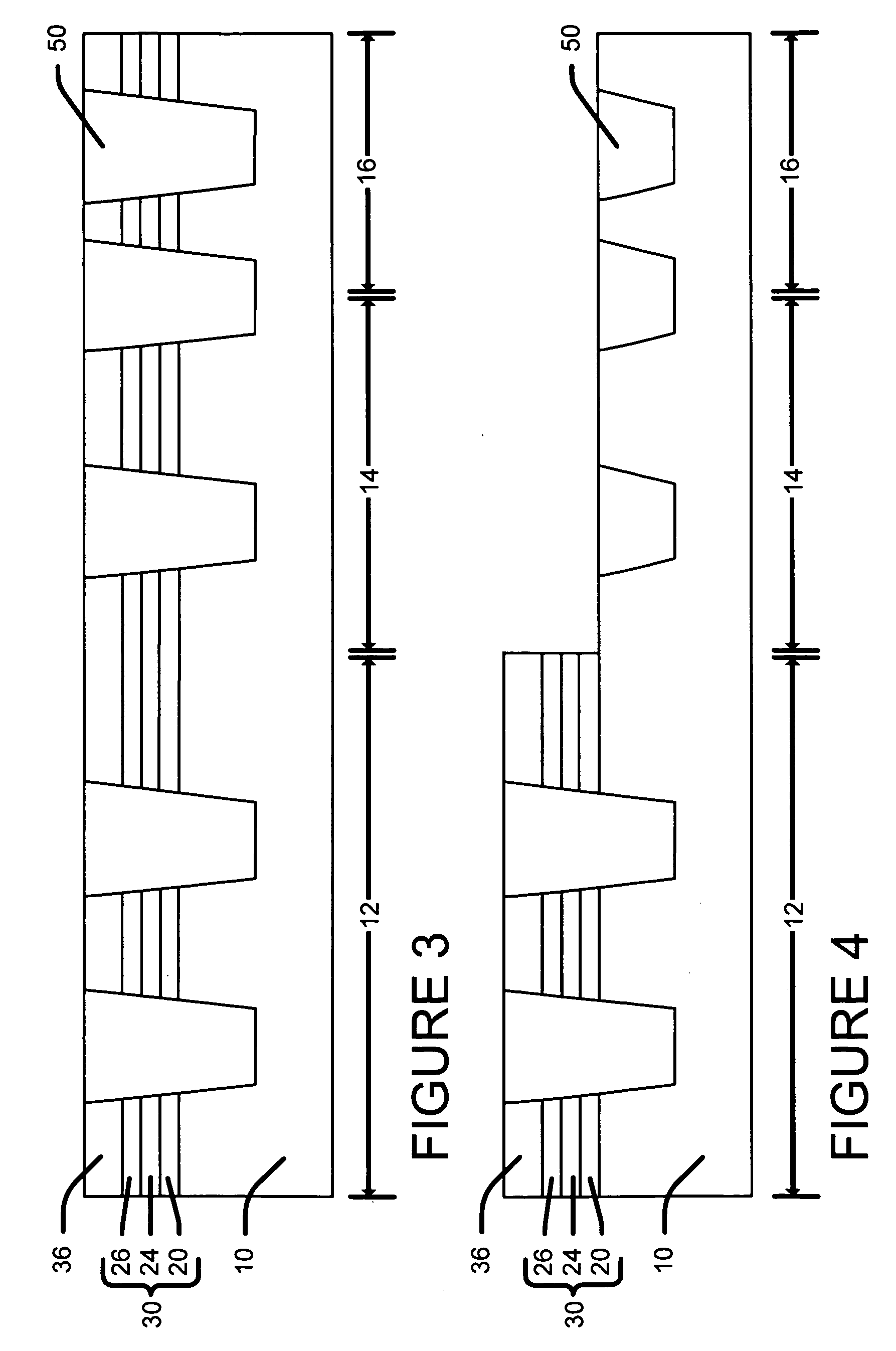
[0036]The first example embodiment provides a structure and a method for the fabrication of a semiconductor device.

[0037]A feature of some example embodiments is to deposit the charge storing film (e.g., ONO) prior to shallow trench isolation (STI) etch and fill process. Instead of pad oxide and pad nitride for normal STI process, in embodiments, the charge storing film (e.g., ONO), gate pad (e.g., poly Pad) and pad nitride film are deposited sequentially, in which ONO and gate pad are used in the SONOS cell. The embodiment's charge storing film (e.g., ONO) quality is improved because the gate pad layer is preferably deposited next after charge storing film deposition. This keeps the charge storing film clean.

[0038]In the example embodiment below the charge storing film is described as a ONO film. It is understood that other film configurations and compositions can be used. The charge storing film can be a multi-layered non-conductive charge storing film.

A...


PUM


Abstract

In an non-limiting example, we provide a substrate having a cell region, and non-cell regions. We form a tunneling dielectric layer, a charge storing layer, a top insulating layer (e.g., ONO), over the substrate. Then we form a conductive pad layer over the top insulating layer. We form isolation trenches in the pad layer, the charge storing layer and the tunneling dielectric layer and into the substrate. We form isolation regions in the isolation trenches. We remove the pad layer, charge storing layer and the tunneling dielectric layer in the non-cell regions. We form a gate layer over the pad layer and the substrate surface. We complete to form the memory (e.g., SONOS) device in the cell region and other devices in the non-cell regions of the substrate.

Description

BACKGROUND OF INVENTION[0001]1) Field of the Invention[0002]Embodiments of this invention relates generally to a structure and method for forming a semiconductor memory device and more particularly to a SONOS memory device.[0003]2) Description of the Prior Art[0004]Semiconductor memory devices in general can be divided into two types: a random access memory (RAM) and a read only memory (ROM). The RAM, such as a dynamic random access memory (DRAM) and a static access memory (SRAM), is fast to input and output data and is volatile such that previously stored data is removed after a predetermined time has passed or power turn-off. Although the ROM keeps data once it is stored, it is slow to input and output data. The ROM includes a Rom, a programmable ROM (PROM), an erasable PROM (EPROM), and an electrically erasable PROM (EEPROM). Recently, there is an increasing demand for EEPROM being capable of electrically programming or removing data. The EEPROM or a cell of a flash memory having...

Claims


Application Information

Patent Timeline
Patent Type & Authority Applications(United States)
IPC IPC(8): H01L21/76
CPCH01L27/11568H01L27/115H10B43/30H10B69/00
Inventor JUNG, SUNG MUNLIM, YOKE LENG LOUISNAGARAD, SRIPADSOHN, DONG KYUNLIU, DONG HUACHEN, XIAO YULOW, RACHEL
Owner CHARTERED SEMICONDUCTOR MANUFACTURING
Features
  • R&D
  • Intellectual Property
  • Life Sciences
  • Materials
  • Tech Scout
  • Unparalleled Data Quality
  • Higher Quality Content
  • 60% Fewer Hallucinations
Learn More