Flash / Phase-Change Memory in Multi-Ring Topology Using Serial-Link Packet Interface

a phase-change memory and serial-link packet interface technology, applied in the field of memory controllers and memory chips, can solve the problems of limiting the number of memory modules that can be chained together, and the module the farthest away from the host's memory controller has a large latency

Inactive Publication Date: 2008-01-17
SUPER TALENT ELECTRONICS
View PDF11 Cites 186 Cited by
  • Summary
  • Abstract
  • Description
  • Claims
  • Application Information

AI Technical Summary

Problems solved by technology

Unfortunately, the module that is the farthest away from the host's memory controller has a large latency since data must be retransmitted by all other modules in the daisy chain.
This latency problem puts a limit on the number of memory modules that can be chained together.

Method used


Image

  • Flash / Phase-Change Memory in Multi-Ring Topology Using Serial-Link Packet Interface
  • Flash / Phase-Change Memory in Multi-Ring Topology Using Serial-Link Packet Interface
  • Flash / Phase-Change Memory in Multi-Ring Topology Using Serial-Link Packet Interface

Examples


Embodiment Construction

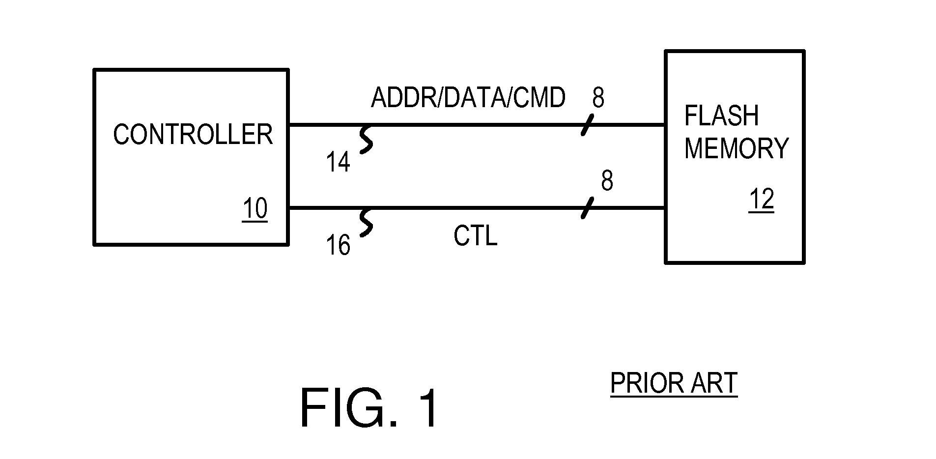
[0029] The present invention relates to an improvement in serial-ring-linked memory systems. The following description is presented to enable one of ordinary skill in the art to make and use the invention as provided in the context of a particular application and its requirements. Various modifications to the preferred embodiment will be apparent to those with skill in the art, and the general principles defined herein may be applied to other embodiments. Therefore, the present invention is not intended to be limited to the particular embodiments shown and described, but is to be accorded the widest scope consistent with the principles and novel features herein disclosed.

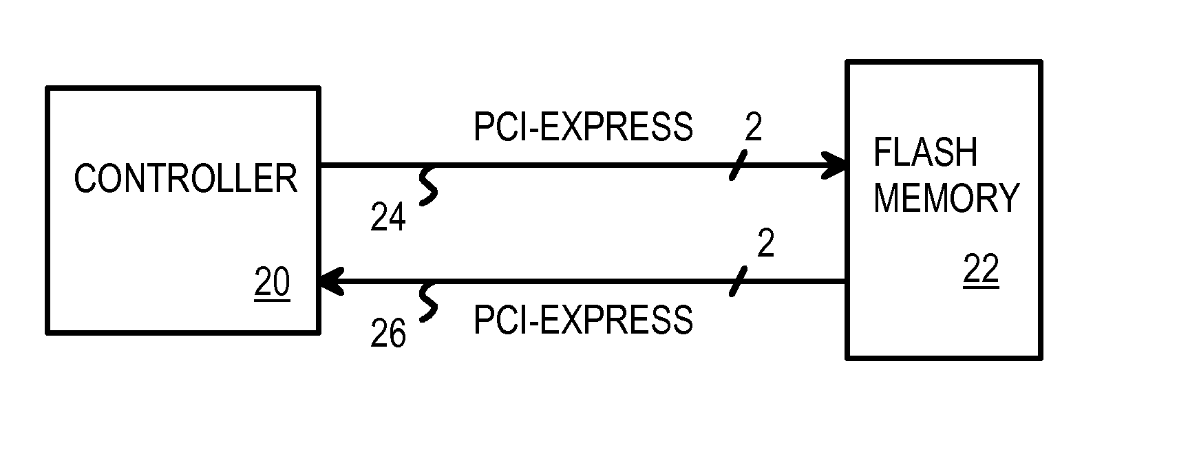
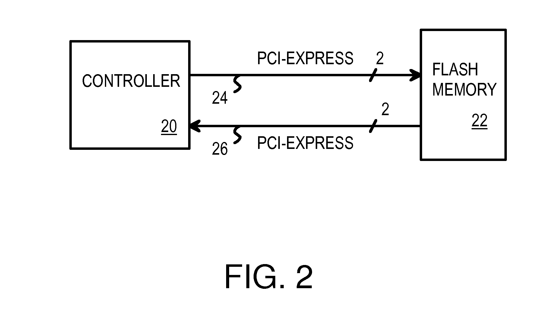
[0030] Serial Link—FIG. 2

[0031]FIG. 2 is a block diagram of a serial interface to a flash-memory chip. Serial flash-memory chip 22 has a serial-bus external interface rather than an 8-bit I / O bus. Controller 20 also uses the serial-bus interface, generating serial-bus packets to access serial flash-memory chip 22. ...


PUM


Abstract

A multi-ring memory controller sends request packets to multiple rings of serial flash-memory chips. Each of the multiple rings has serial flash-memory chips with serial links in a uni-directional ring. Each serial flash-memory chip has a bypassing transceiver with a device ID checker that bypasses serial packets to a clock re-synchronizer and bypass logic for retransmission to the next device in the ring, or extracts the serial packet to the local device when an ID match occurs. Serial packets pass through all devices in the ring during one round-trip transaction from the controller. The average latency of one round is constant for all devices on the ring, reducing data-dependent performance, since the same packet latency occurs regardless of the data location on the ring. The serial links can be a Peripheral Component Interconnect (PCI) Express bus. Packets have modified-PCI-Express headers that define the packet type and data-payload length.

Description

RELATED APPLICATION [0001] This application is a continuation-in-part (CIP) of the co-pending application for “PCI Express-Compatible Controller and Interface for Flash Memory”, U.S. Ser. No. 10 / 803,597, filed Mar. 17, 2004. This application is also related to “Serial Interface to Flash Memory Chip using PCI-Express-Like Packets and Packet Data for Partial-page Writes”, U.S. Pat. No. 7,130,958, filed Feb. 9, 2004.FIELD OF THE INVENTION [0002] This invention relates to memory systems, and more particularly to a memory controller and memory chips that are connected together by one or more rings of high-speed serial links. BACKGROUND OF THE INVENTION [0003] Flash memory has gained wide acceptance for its non-volatile storage, which is ideal for portable devices that may lose power, since the data is not lost when stored in the flash memory. Flash memories are constructed from electrically-erasable programmable read-only memory (EEPROM) cells. [0004] Rather than use a randomly-addressab...

Claims


Application Information

Patent Timeline
Patent Type & Authority Applications(United States)
IPC IPC(8): G06F12/00
CPCG06F13/1684G11C2216/30G11C16/102G11C13/0004
Inventor CHOW, DAVID Q.LEE, CHARLES C.YU, FRANK
Owner SUPER TALENT ELECTRONICS
Why Eureka
Try Eureka