Dual work function metal gate structure and related method of manufacture

a metal gate structure and dual work technology, applied in the field of semiconductor devices having a dual metal gate structure, can solve the problems of ambiguity in application, conventional practices are too limited in their application,

Active Publication Date: 2008-01-24
SAMSUNG ELECTRONICS CO LTD
View PDF11 Cites 33 Cited by
  • Summary
  • Abstract
  • Description
  • Claims
  • Application Information

AI Technical Summary

Benefits of technology

[0021] The conventional practices are too limited in their application and suffer from a certain amount of ambiguity in application. In contrast, the invention provides improved methods for adjusting the work function of a metal layer and corresponding semiconductor devices.

Problems solved by technology

The conventional practices are too limited in their application and suffer from a certain amount of ambiguity in application.

Method used


Image

  • Dual work function metal gate structure and related method of manufacture
  • Dual work function metal gate structure and related method of manufacture
  • Dual work function metal gate structure and related method of manufacture

Examples


Embodiment Construction

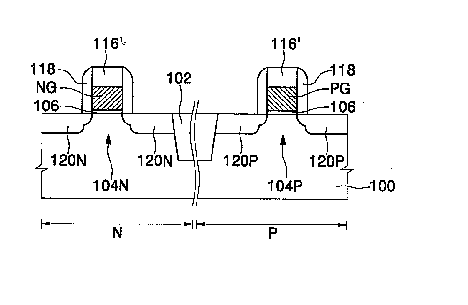
[0038] Exemplary embodiments of the invention are described below with reference to the corresponding drawings. These embodiments are presented as teaching examples. The actual scope of the invention is defined by the claims that follow. Those of ordinary skill in the art will appreciate that the term “on” as used in relation to the formation of various semiconductor layers and regions describes a relationship in which one layer / region is directly on another, or in which the one layer / region is on another, but one or more intervening layers and / or regions separate the two layer / regions.

[0039] Among other aspects, the exemplary embodiments of the invention described below illustrate the formation and composition of dual metal gate structures, and related constituent metal gate electrodes. The term “dual” in this context refers to separate gate structures adapted for use with different transistor types. Transistors used in the formation of semiconductor devices are classified as bein...


PUM

PropertyMeasurementUnit
work functionaaaaaaaaaa

Abstract

A semiconductor device and related methods of manufacture are disclosed in which dual work function metal gate electrodes are formed from a single metal layer by doping the metal layer with carbon and/or fluorine.

Description

CROSS-REFERENCE TO RELATED APPLICATION [0001] This is a divisional of application Ser. No. 11 / 192,288 filed on Jul. 29, 2005, which is incorporated herein by reference in its entirety.BACKGROUND OF THE INVENTION [0002] 1. Field of the Invention [0003] The present invention relates generally to semiconductor devices and related methods of manufacture. More particularly, the invention relates to semiconductor devices having a dual metal gate structure and related methods of manufacture. [0004] 2. Description of the Related Art [0005] Constant demand for evermore densely integrated semiconductor devices, including the demand for semiconductor memory devices of constantly increasing capacity, has resulted in relentless pressure to reduce the size of the constituent components forming contemporary semiconductor devices. For example, the physical dimensions of nearly every constituent component in conventional Complementary Metal Oxide Semiconductor (CMOS) devices have been dramatically r...

Claims


Application Information

Patent Timeline
Patent Type & Authority Applications(United States)
IPC IPC(8): H01L29/78
CPCH01L21/265H01L21/28088H01L29/7833H01L29/4958H01L29/6659H01L21/823842
Inventor KIM, MIN-JOOJUNG, HYUNG-SUKLEE, JONG-HOHAN, SUNGKEE
Owner SAMSUNG ELECTRONICS CO LTD
Why Eureka
Try Eureka