Plasma based ion implantation apparatus

a technology of ion implantation and plasma, which is applied in the direction of electrical equipment, basic electric elements, electric discharge tubes, etc., can solve the problems of reducing process efficiency and productivity, high manufacturing cost, and reducing the efficiency of ion implantation, so as to achieve the effect of suppressing arcing

Inactive Publication Date: 2008-01-31
SAMSUNG ELECTRONICS CO LTD
View PDF17 Cites 17 Cited by
  • Summary
  • Abstract
  • Description
  • Claims
  • Application Information

AI Technical Summary

Benefits of technology

[0048]The upper chamber may be configured to prevent an electric field used to generate the plasma from propagating into the lower chamber to suppress arcing in the lower chamber.
[0049]The apparatus may further include an antenna coil to generate plasma in the upper chamber, disposed to surround the upper chamber, and a conductor plate disposed inside t

Problems solved by technology

Thus, the conventional ion beam based ion implantation apparatus suffers from problems of a complicated structure, a large volume, and a high price causing high manufacturing costs.
However, the conventional ion beam based ion implantation apparatus has a problem in that, as the energy of the ions decreases, a divergence of the ion beams caused by repulsion between the ions becomes significant, causing a reduction of ion implantation efficiency.
In other words, in order to satisfy requirements for the ion implantation process to manufacture highly integrated semico

Method used


Image

  • Plasma based ion implantation apparatus
  • Plasma based ion implantation apparatus
  • Plasma based ion implantation apparatus

Examples


Embodiment Construction

[0061]Reference will now be made in detail to the embodiments of the present general inventive concept, examples of which are illustrated in the accompanying drawings, wherein like reference numerals refer to the like elements throughout. The embodiments are described below in order to explain the present general inventive concept by referring to the figures.

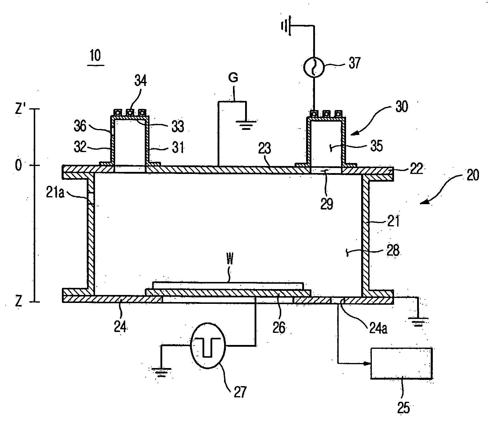
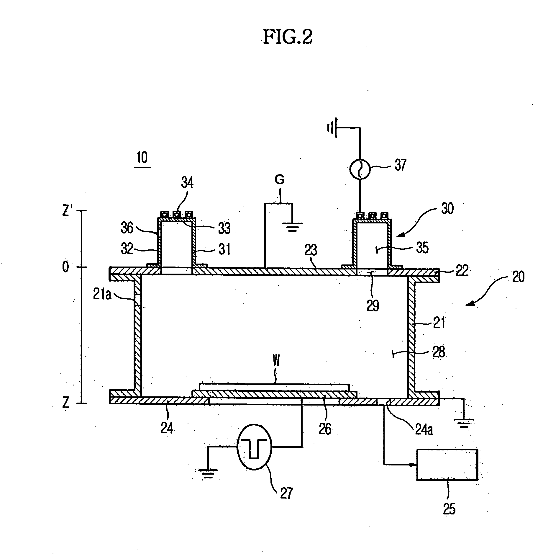
[0062]FIG. 2 is a cross-sectional view illustrating a plasma based ion implantation apparatus according to an embodiment of the present general inventive concept, and FIG. 3 is a cut-away perspective view illustrating the plasma based ion implantation apparatus of FIG. 2.

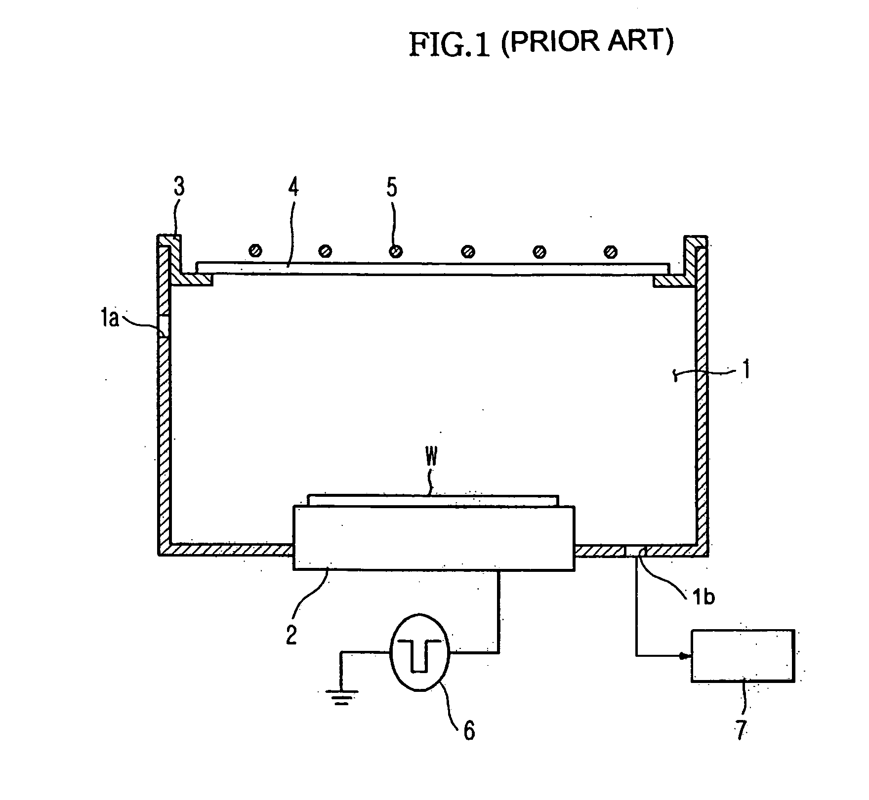
[0063]A plasma based ion implantation apparatus refers to a semiconductor manufacturing apparatus which forces positive ions of plasma to collide with and be implanted into a surface of a target, such as a wafer, through application of high voltage pulses to the target after forming the plasma from an implantation object material, which is introduced in a gas st...


PUM


Abstract

A plasma based ion implantation apparatus. The apparatus includes a first chamber in which plasma is generated, a coil antenna to generate the plasma in the first chamber, a second chamber in which ions of the plasma are implanted into a target, the second chamber having an incoming port through which the plasma is diffused from the first chamber to the second chamber, a power source to supply high voltage power to the target in the second chamber, and a grounded conductor positioned to face the target seated on the seating table. The first chamber is formed with a ring shape opening of a predetermined width at an upper periphery of the second chamber to communicate with the second chamber.

Description

CROSS-REFERENCE TO RELATED APPLICATIONS[0001]This application claims priority under 35 U.S.C. §119(a) from Korean Patent Application No. 2006-0070037, filed on Jul. 25, 2006 in the Korean Intellectual Property Office, the disclosure of which is incorporated herein in its entirety by reference.BACKGROUND OF THE INVENTION[0002]1. Field of the Invention[0003]The present general inventive concept relates to an ion implantation apparatus, and more particularly to a plasma based ion implantation apparatus.[0004]2. Description of the Related Art[0005]Ion implantation is a materials engineering process by which impurity atoms with a high kinetic energy are implanted into a wafer surface through an ionization and acceleration of impurities desired to be implanted into the wafer.[0006]In semiconductor device fabrication, an ion implantation process serves to create characteristics of electronic elements by accelerating and implanting ionized impurities into a portion of the wafer connected to...

Claims


Application Information

Patent Timeline
IPC IPC(8): G21K5/08
CPCH01J37/32412H01J37/321H01L21/265H01L21/3065
Inventor LEE, YOUNG DONGTOLMACHEV, YURIVOLYNETS, VLADIMIRPASHKOVSKIY, VASILY
Owner SAMSUNG ELECTRONICS CO LTD
Why Eureka
Try Eureka