Nonvolatile semiconductor memory device

a semiconductor memory and non-volatile technology, applied in static storage, digital storage, instruments, etc., can solve the problems of inability to read in the worse case, inability to record information, and inability to completely lose stored data, so as to achieve the effect of suppressing the resistance change of the variable resistance element due to the reading disturban

Inactive Publication Date: 2008-01-31
SHARP KK +1
View PDF8 Cites 35 Cited by
  • Summary
  • Abstract
  • Description
  • Claims
  • Application Information

AI Technical Summary

Benefits of technology

[0031]According to the nonvolatile semiconductor memory device having the third characteristics, even in the case of the 1R-type memory cell comprising the variable resistance element only, since the reading voltage is applied to the variable resistance element of the selected memory cell by the forward bias, the resistance change of the variable resistance element due to the reading disturbance can be effectively suppressed even in the case where the memory cell is selected by the row or column and the reading disturbance becomes prominent especially.
[0032]According to the nonvolatile semiconductor memory device having the fourth or fifth characteristics, even in the case of the 1T/1R-type memory cell having the series circuit comprising the variable resistance element and the cell-access t

Problems solved by technology

In addition, since the resistance value in the above reading operation tends to increase, when the same reading operation is continued, the resistance state is changed from the low resistance state to the high resistance state, so that recorded information is lost.
Especially, the resistance value of the variable resistance element

Method used


Image

  • Nonvolatile semiconductor memory device
  • Nonvolatile semiconductor memory device
  • Nonvolatile semiconductor memory device

Examples


first embodiment

[0059]FIG. 5 shows the schematic constitution of a device of the present invention according to a first embodiment. As shown in FIG. 5, the device of the present invention comprises a bit line decoder 16, a word line decoder 17, a voltage switch circuit 22, a readout circuit 23, a voltage generation circuit 24, and a control circuit 20 in the vicinity of a memory cell array 25 in which 1R-type memory cells are arranged in a matrix state.

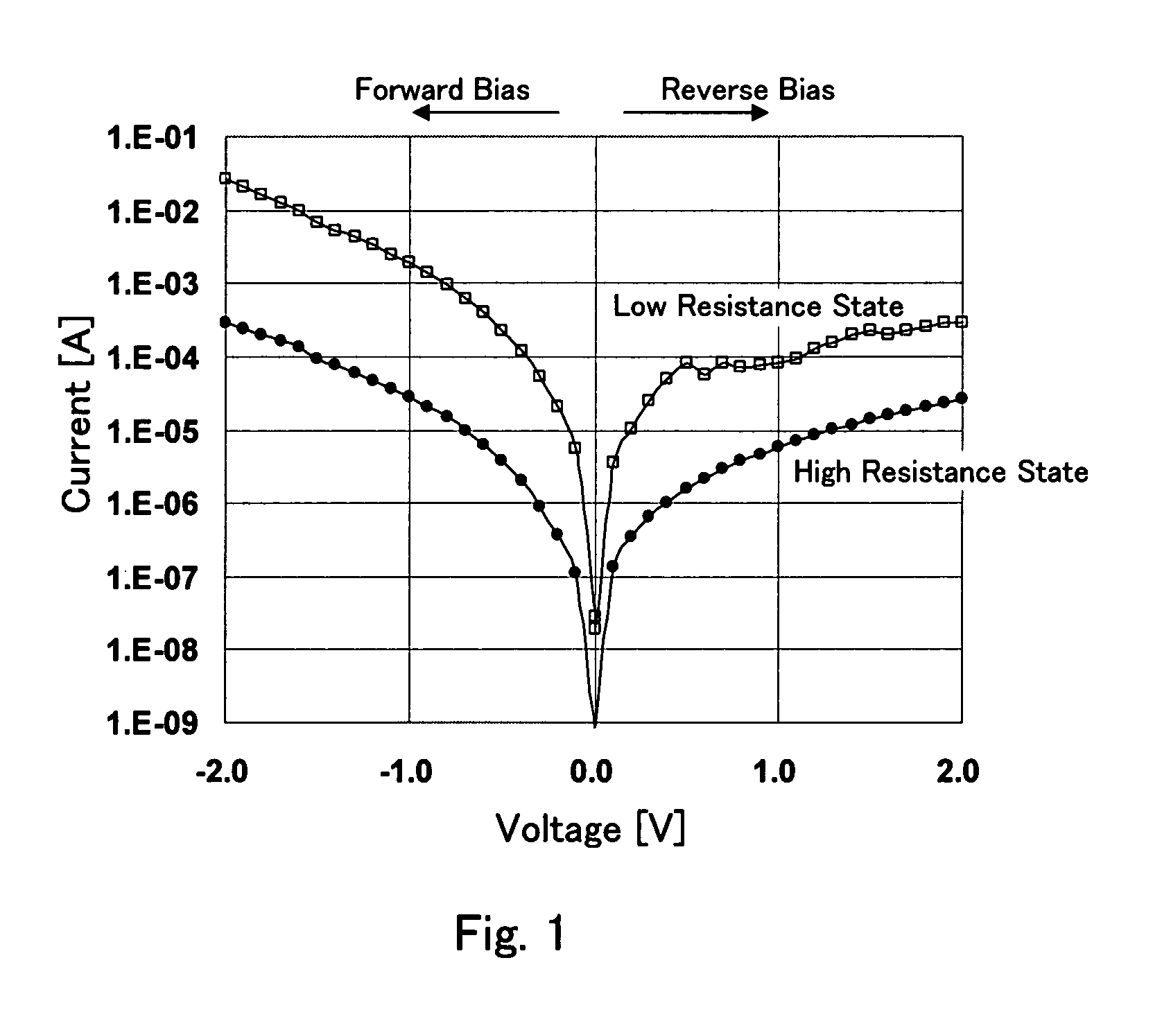
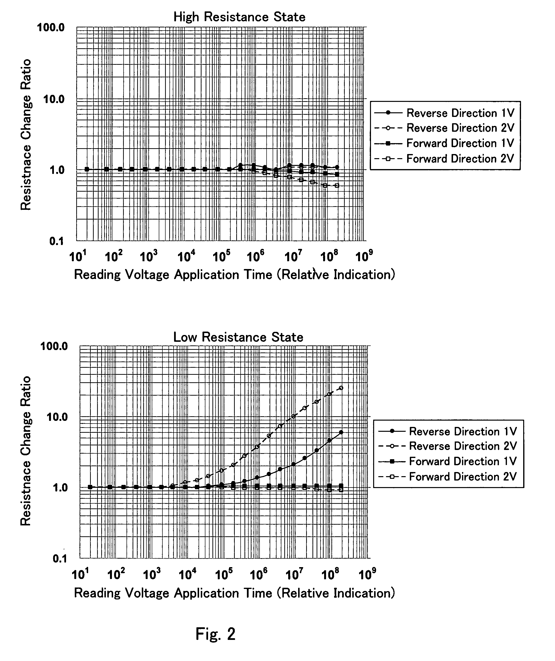
[0060]As shown in FIG. 6, the memory cell array 25 is provided such that each of m×n memory cells 1 is disposed at each intersection of m bit lines extending in a column direction (corresponding to a column selection line) BL1 to BLm and n word lines extending in a row direction (corresponding to a row selection line) WL1 to WLn. The variable resistance element 3 constituting each memory cell 1 has the rectifying characteristics and it is connected to the word line and the bit line such that the current flowing from the bit line to the word line beco...

second embodiment

[0070]Although the description has been made of the case where the memory cell is the 1R-type memory cell in the first embodiment, a description will be made of a case where the memory cell is an 1T / 1R-type memory cell hereinafter.

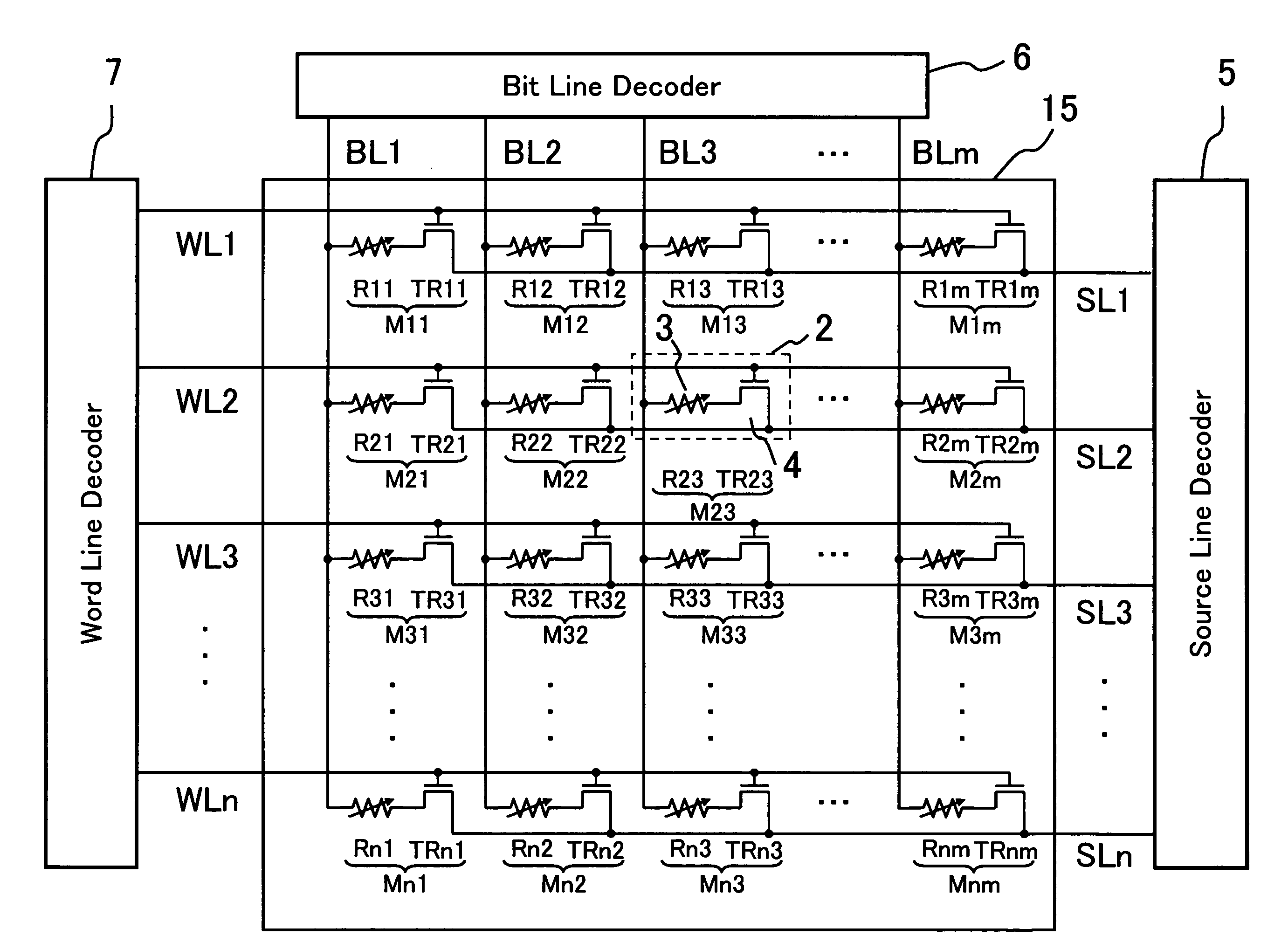
[0071]FIG. 10 shows the schematic constitution of a device of the present invention according to a second embodiment. As shown in FIG. 10, the device of the present invention comprises a word line decoder 7, a bit line decoder 6, a source line decoder 5, a voltage switch circuit 12, a readout circuit 13, a voltage generation circuit 14, and a control circuit 10 in the vicinity of a memory cell array 15 in which 1T / 1R-type memory cells are arranged in a matrix state. A specific memory cell in the memory cell array 15 corresponding to an address inputted from an address line 8 to the control circuit 10 is selected by the bit line decoder 6, the source line decoder 5 and the word line decoder 7 and the data is programmed, erased or read and the data is stored...

third embodiment

[0083]FIG. 14 shows the schematic constitution of a device of the present invention according to the third embodiment. As shown in FIG. 14, although the device of the present invention has the same constitution as that of the 1R-type memory cell basically, since the memory cell comprises a series circuit consisting of a variable resistance element and a cell-access diode, it is necessary to turn on the cell-access diode of the selected memory cell in the reading operation, so that its voltage applying condition is different from that of the 1R-type memory cell. As shown in FIG. 14, the device of the present invention comprises a bit line decoder 26, a word line decoder 27, a voltage switch circuit 32a, a readout circuit 33a, a voltage generation circuit 34a, and a control circuit 30a in the vicinity of a memory cell array 35a in which 1D / 1R-type memory cells are arranged in a matrix state.

[0084]As shown in FIG. 15, the memory cell array 35a is constituted such that each of m×n memor...


PUM


Abstract

A nonvolatile semiconductor memory device comprises a memory cell including a variable resistance element changing its electric resistance by voltage application and having current-voltage characteristics in which a positive bias current flowing when a positive voltage is applied from one electrode as a reference electrode to the other electrode through an incorporated rectifier junction is larger than a negative bias current, a memory cell selection circuit for selecting the memory cell from the memory cell array, a voltage supply circuit for supplying a voltage to the memory cell so that a predetermined positive voltage corresponding to the reading operation is applied to the other electrode of the variable resistance element, in the reading operation, and a readout circuit for detecting the amount of the positive bias current and reading the information stored in the selected memory cell, in order to suppress the reading disturbance of the memory cell.

Description

CROSS REFERENCE TO RELATED APPLICATION[0001]This Nonprovisional application claims priority under 35 U.S.C. § 119(a) on Patent Application No. 2006-206678 filed in Japan on 28 Jul., 2006 the entire contents of which are hereby incorporated by reference.BACKGROUND OF THE INVENTION[0002]1. Field of the Invention[0003]The present invention relates to a nonvolatile semiconductor memory device having a memory cell array in which memory cells each comprising a variable resistance element storing information by the change of an electric resistance are arranged in a row direction and a column direction, and more particularly, to a technique for preventing and suppressing the deterioration of stored data due to the reading operation of the memory cell array.[0004]2. Description of the Related Art[0005]Recently, there has been proposed a variable resistance type of memory element (referred to as the variable resistance element hereinafter) having a two-terminal structure in which a metal oxid...

Claims


Application Information

Patent Timeline
IPC IPC(8): G11C11/00
CPCG11C8/10G11C11/16G11C13/0007G11C2213/72G11C13/0069G11C2013/009G11C2213/31G11C13/004
Inventor TAMAI, YUKIOSAWA, AKIHITO
Owner SHARP KK
Why Eureka
Try Eureka