SELF-ALIGNED PROCESS FOR NANOTUBE/NANOWIRE FETs

a nanotube and nanowire technology, applied in the field of semiconductor structure, can solve the problem of not having a self-aligning process comparable to conventional cmos technology

Inactive Publication Date: 2008-01-31
GLOBALFOUNDRIES INC
View PDF15 Cites 12 Cited by
  • Summary
  • Abstract
  • Description
  • Claims
  • Application Information

AI Technical Summary

Problems solved by technology

However, there is no known self-aligned process comparable to conventional CMOS technology.

Method used


Image

  • SELF-ALIGNED PROCESS FOR NANOTUBE/NANOWIRE FETs
  • SELF-ALIGNED PROCESS FOR NANOTUBE/NANOWIRE FETs
  • SELF-ALIGNED PROCESS FOR NANOTUBE/NANOWIRE FETs

Examples


Embodiment Construction

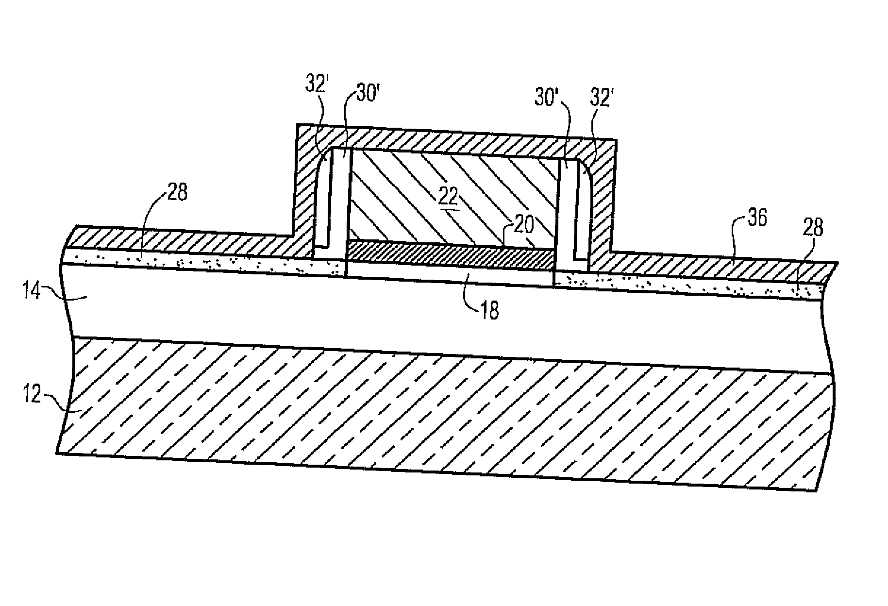
[0034] The present invention, which provides a one-dimensional nanostructure-containing FET and a method of fabricating the same, will now be described in greater detail by referring to the drawings that accompany the present application. The various drawings of the present invention are provided for illustrative purposes and thus they are not drawn to scale. Also, the drawings depict the presence of a single gate region; the term “gate region” is used herein to denote the gate, gate electrode and underlying device channel. Although a single gate region is depicted and described, the present invention also contemplates forming a plurality of such gate regions and thus a plurality of one-dimensional nanostructure-containing FETs on a surface of a substrate.

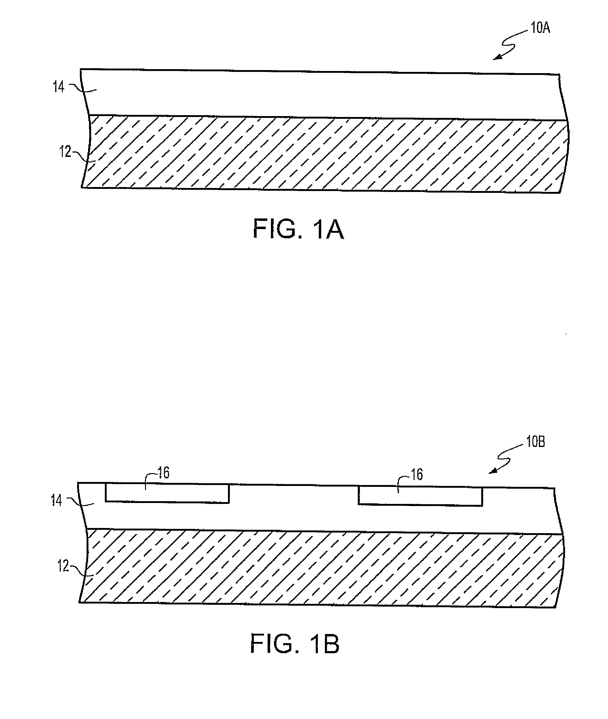
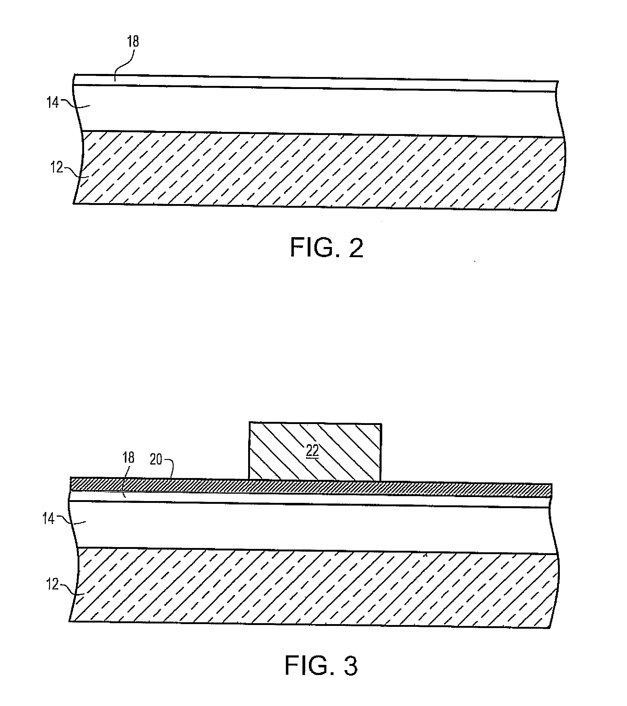
[0035] The present invention begins with first providing the initial substrate shown in either FIG. 1A or FIG. 1B. The initial substrate 10A shown in FIG. 1A comprises a semiconductor layer 12 which includes a dielectric layer 14 ...


PUM

PropertyMeasurementUnit
temperatureaaaaaaaaaa
thicknessaaaaaaaaaa
thicknessaaaaaaaaaa

Abstract

A complementary metal oxide semiconductor (CMOS) device, e.g., a field effect transistor (FET), that includes at least one one-dimensional nanostructure that is typically a carbon-based nanomaterial, as the device channel, and a metal carbide contact that is self-aligned with the gate region of the device is described. The present invention also provides a method of fabricating such a CMOS device.

Description

RELATED APPLICATIONS [0001] This application is a divisional application of U.S. Ser. No. 11 / 031,168, filed Jan. 7, 2005.FIELD OF THE INVENTION [0002] The present invention relates to a semiconductor structure and a method of fabricating the same. More particularly, the present invention relates to a complementary metal oxide semiconductor (CMOS) device, e.g., a field effect transistor (FET), that comprises at least one one-dimensional nanostructure that is typically a carbon-based nanomaterial, as the device channel, and a metal carbide contact that is self-aligned with the gate region of the device, i.e., aligned to an edge of the gate region. The present invention also provides a method of fabricating such a CMOS device. BACKGROUND OF THE INVENTION [0003] In the field of molecular nanoelectronics, few materials show as much promise as one-dimensional nanostructures, and in particular carbon nanotubes that comprise hollow cylinders of graphite that have a diameter of a few Angstro...

Claims


Application Information

Patent Timeline
Patent Type & Authority Applications(United States)
IPC IPC(8): H01L21/336
CPCB82Y10/00H01L29/0665H01L29/0673H01L29/665Y10S977/938H01L29/7833H01L51/0048H01L51/0541Y10S977/847H01L29/6656H10K85/221H10K10/464H01L29/775B82Y40/00H10K99/00
Inventor AVOURIS, PHAEDONCARRUTHERS, ROY A.CHEN, JIADETAVERNIER, CHRISTOPHE G.M.M.LAVOIE, CHRISTIANWONG, HON-SUM PHILIP
Owner GLOBALFOUNDRIES INC
Why Eureka
Try Eureka