Phase change memory cell and method and system for forming the same

a phase change memory and memory cell technology, applied in digital storage, instruments, electrical apparatus, etc., can solve problems such as degrading integrated circuit performance, and achieve the effects of preventing undercutting into phase change materials, low reactivity, and easy removal

Active Publication Date: 2008-01-31
SAMSUNG ELECTRONICS CO LTD
View PDF8 Cites 12 Cited by
  • Summary
  • Abstract
  • Description
  • Claims
  • Application Information

AI Technical Summary

Benefits of technology

[0024]In this manner, by using the low-reactivity halogen element such as bromine in HBr or iodine in HI during etching of the top electrode material, undercutting into the phase change material is prevented. In addition, the composition of the phase change material is not significantly altered after such etching of the top electrode material. Furthermore, the low-reactivity halogen by-product may be more easily removed and has relatively low reactivity such that a heat budget may not be required during subsequent heating process steps.

Problems solved by technology

Such diffusion may degrade integrated circuit performance, and such diffusion imposes a heat budget for minimizing such diffusion during subsequent heating processes.

Method used


Image

  • Phase change memory cell and method and system for forming the same
  • Phase change memory cell and method and system for forming the same
  • Phase change memory cell and method and system for forming the same

Examples


Embodiment Construction

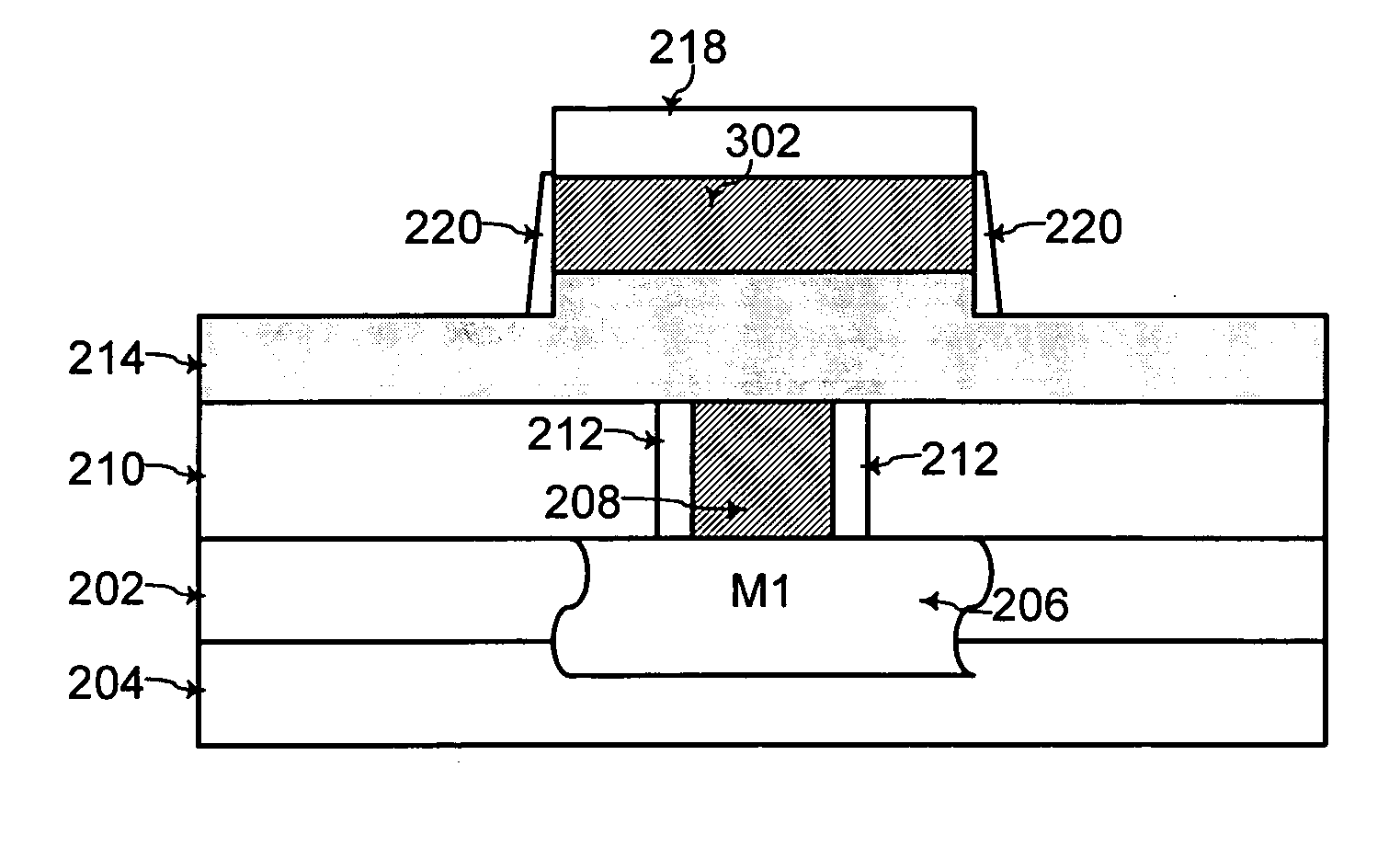
[0044]FIGS. 7, 8, 9, 11, 12, 13, and 14 show cross-sectional views during fabrication of phase change memory cells according to embodiments of the present invention. FIGS. 16, 18, and 20 show flow-charts of steps during fabrication of phase change memory cells according to embodiments of the present invention.

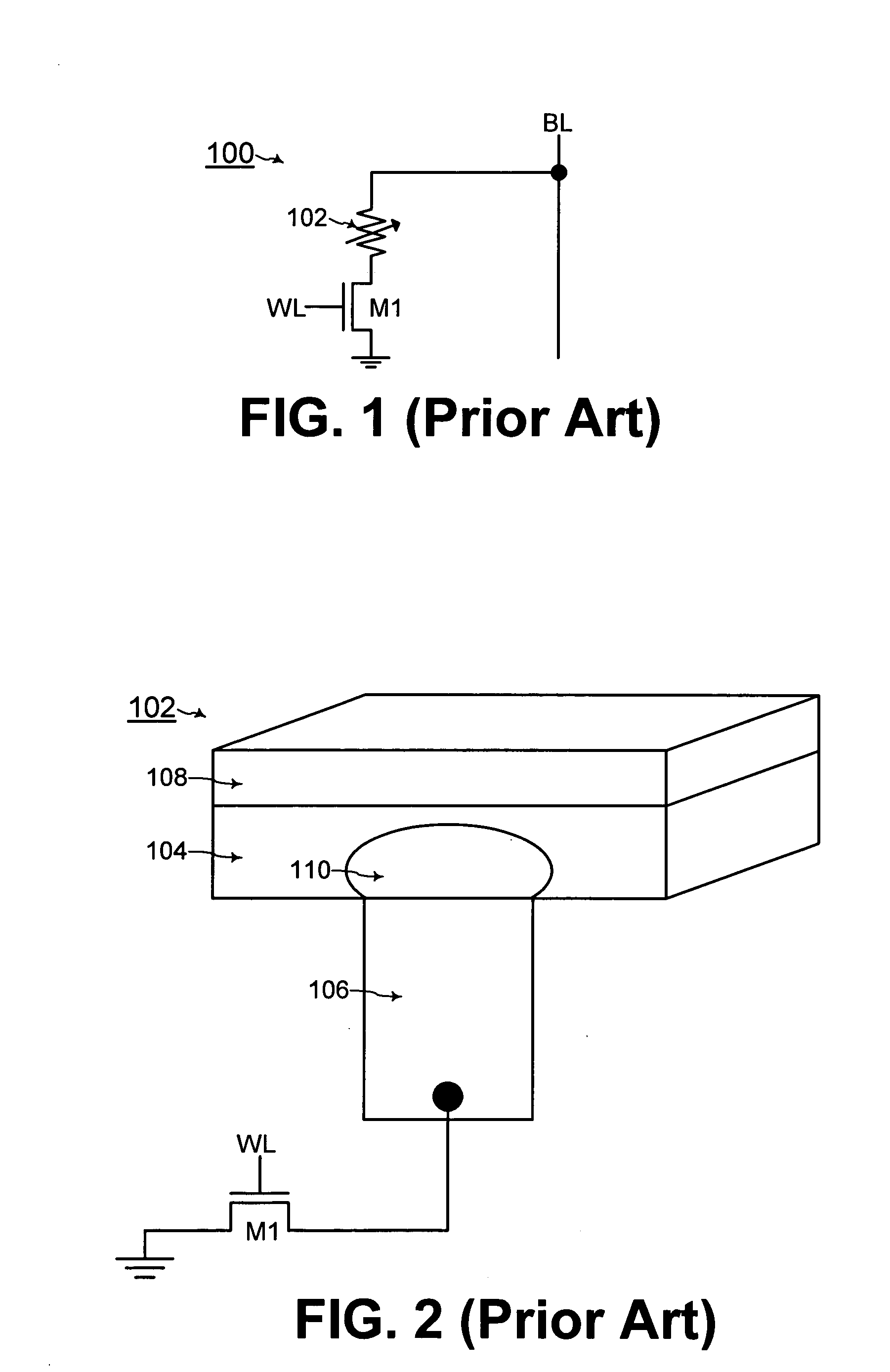
[0045]Referring to FIG. 7, at least one inter-level material 202 is deposited on a semiconductor substrate 204. In one example embodiment of the present invention, a transistor M1 such as the field effect transistor M1 of FIG. 1 for example associated with the phase change memory cell is formed with the semiconductor substrate 204 and the at least one inter-level material 202. The semiconductor substrate 204 is a silicon wafer in one example embodiment of the present invention.

[0046]Further referring to FIG. 7, a bottom electrode 208 is formed as a plug in a layer of insulating material 210 formed on the at least one inter-level material 202 (steps 302, 402, and 502 of FIGS. 16...


PUM


Abstract

For fabricating a phase change memory cell, a layer of phase change material and a layer of a first electrode material are deposited. In addition, the first electrode material is patterned using an etchant including a low-reactivity halogen element such as bromine or iodine to form a first electrode. By using the low-reactivity halogen element, change to the composition of the phase change material and formation of undercut and deleterious halogen by-product are avoided.

Description

CROSS-REFERENCE TO RELATED APPLICATION(S)[0001]The present application claims priority under 35 U.S.C. §119 to Korean Patent Application No. 2006-72195, filed on Jul. 31, 2006, which is incorporated herein by reference in its entirety.TECHNICAL FIELD[0002]The present invention relates generally to phase change memory devices, and more particularly, to patterning an electrode material using an etchant including a low-reactivity halogen element for preserving the integrity of the phase change material in a phase change memory cell.BACKGROUND OF THE INVENTION[0003]FIG. 1 shows a circuit diagram of a phase change memory cell 100 including a variable resistor 102 and a field effect transistor M1, as known in the prior art. The variable resistor 102 has one terminal coupled to a bit-line of a phase change memory device. The variable resistor 102 has another terminal coupled to a drain of the field effect transistor M1. The gate of the field effect transistor M1 is coupled to a word-line o...

Claims


Application Information

Patent Timeline
Patent Type & Authority Applications(United States)
IPC IPC(8): H01L21/311H01L21/8238H01L21/20H01L21/302
CPCH01L45/06H01L45/1233H01L45/1675H01L45/144H01L45/143H10N70/231H10N70/826H10N70/8825H10N70/8828H10N70/063G11C13/0004
Inventor CHO, HONGCHUNG, SEUNG-PILKIM, YOUNG-JAE
Owner SAMSUNG ELECTRONICS CO LTD
Why Eureka
Try Eureka