Through-hole vertical semiconductor devices or chips

a technology of semiconductor devices and chips, applied in semiconductor/solid-state device manufacturing, semiconductor devices, electrical equipment, etc., can solve the problems of complex packaging process, high cost, and high cost, and achieve the effect of reducing series electrical resistance, improving heat dissipation efficiency, and reducing forward voltag

Inactive Publication Date: 2008-02-07
JING PENG +2
View PDF1 Cites 82 Cited by
  • Summary
  • Abstract
  • Description
  • Claims
  • Application Information

AI Technical Summary

Benefits of technology

[0019]The quantities and area of cross section of the through-hole-metal-plugs are pre-determined. The advantages of using plurality and larger cross section area of through-hole-metal-plugs are the following: (1) improving the heat dissipation efficiency further; (2) decreasing series electrical resistance and, thus, reducing the forward voltage and generating less heat.

Problems solved by technology

However, (1) technical and manufacturing issues (including heat dissipation and yield) need to be resolved; (2) performance and reliability need to be continuously improved; (3) products become smaller, thinner and lighter.
Wire bonding causes reliability issue, thicker packages and complicated packaging process.
Also burn-in process has to be done after packaging the chips, which causes uncertainty of chip quality before packaging.
Once the chip is not qualified, then the whole package is failed and hard to re-work, and the cost is increasing.

Method used


Image

  • Through-hole vertical semiconductor devices or chips
  • Through-hole vertical semiconductor devices or chips
  • Through-hole vertical semiconductor devices or chips

Examples


first embodiment

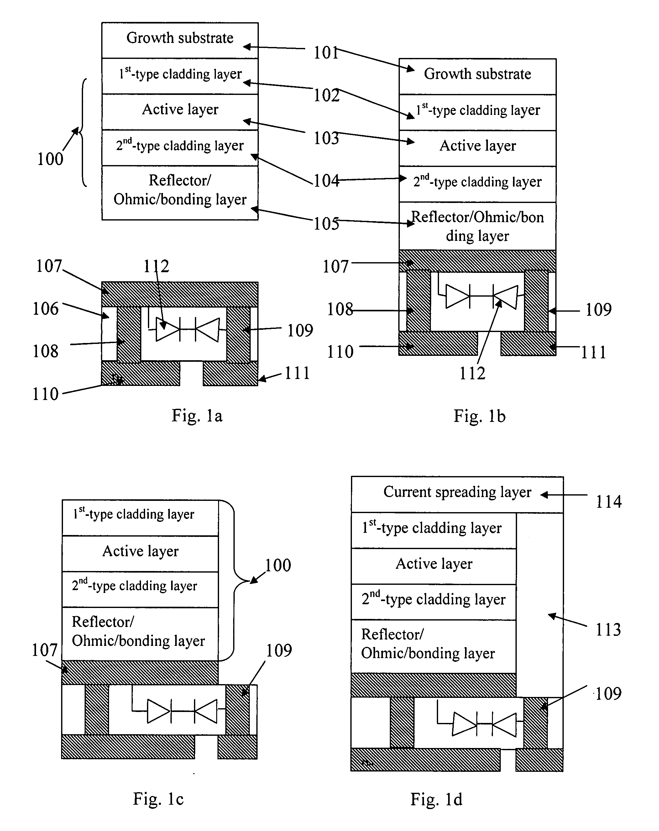
[0051]FIG. 1 shows first embodiment of a method manufacturing through-hole vertical semiconductor devices or chips with built-in static protection diodes. FIG. 1a: providing a semiconductor epitaxial wafer comprising: epitaxial layer 100 growing on growth substrate 101. Normally there is a buffer layer growing between growth substrate 101 and epitaxial layer 100. Since the buffer layer will be removed with growth substrate 101, FIG. 1 does not show the buffer layer. Epitaxial layer 100 comprises first-type cladding layer 102, active layer 103, second-type cladding layer 104. Electrically conductive reflector / Ohmic / bonding layer 105 is deposited on second-type cladding layer 104. The functions of reflector / Ohmic / bonding layer 105 are the following: (1) for LED, reflecting light, forming Ohmic contact, and bonding to the supporting wafer; (2) for other semiconductor devices or chips, forming Ohmic contact and bonding to the supporting wafer.

[0052]The structure of an active layer is se...

second embodiment

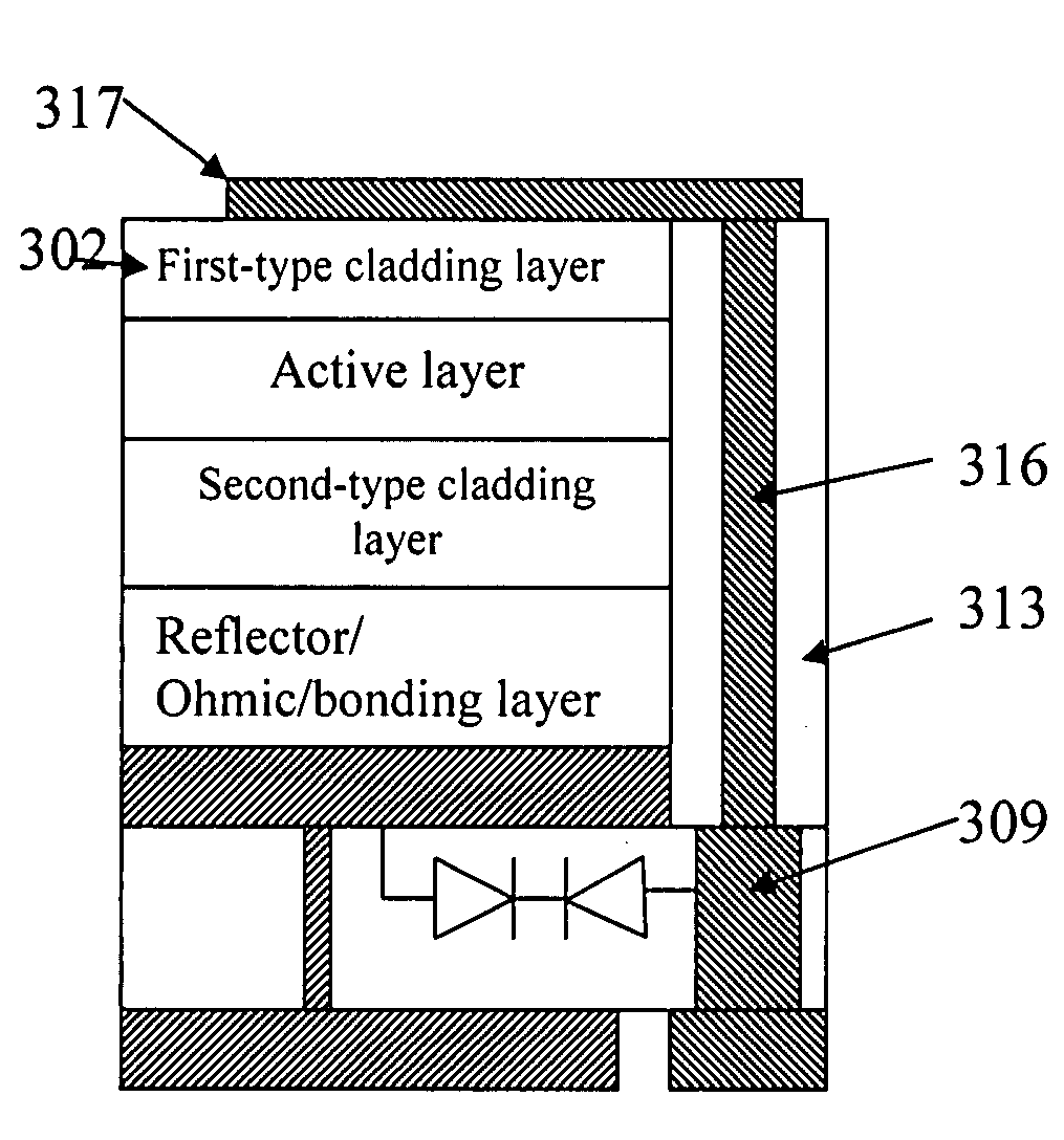
[0062]FIG. 3a to FIG. 3c shows second embodiment of method manufacturing through-hole vertical semiconductor devices or chips with built-in static protection diodes. Firstly repeating the process flow steps of FIG. 1a to FIG. 1c, then, performing the following process flow steps (FIG. 3a to 3c).

[0063]FIG. 3a: forming protection-plug 313 on the exposed surface of through-hole-metal-plug 309.

[0064]FIG. 3b: etching protection-plug 313 at pre-determined positions until the top surface of through-hole-metal-plug 309 exposed to form half-through-hole 314.

[0065]FIG. 3c: forming half-through-hole-metal-plug 316 in half-through-hole 314. Half-through-hole-metal-plug 316 is electrically connected to through-hole-metal-plug 309. Depositing patterned electrode 317 on the top surfaces of both first-type cladding layer 302 and protection-plug 313. Patterned electrode 317 is electrically connected to half-through-hole-metal-plug 316.

[0066]Note: optimizing the pattern of patterned electrode 317, th...

third embodiment

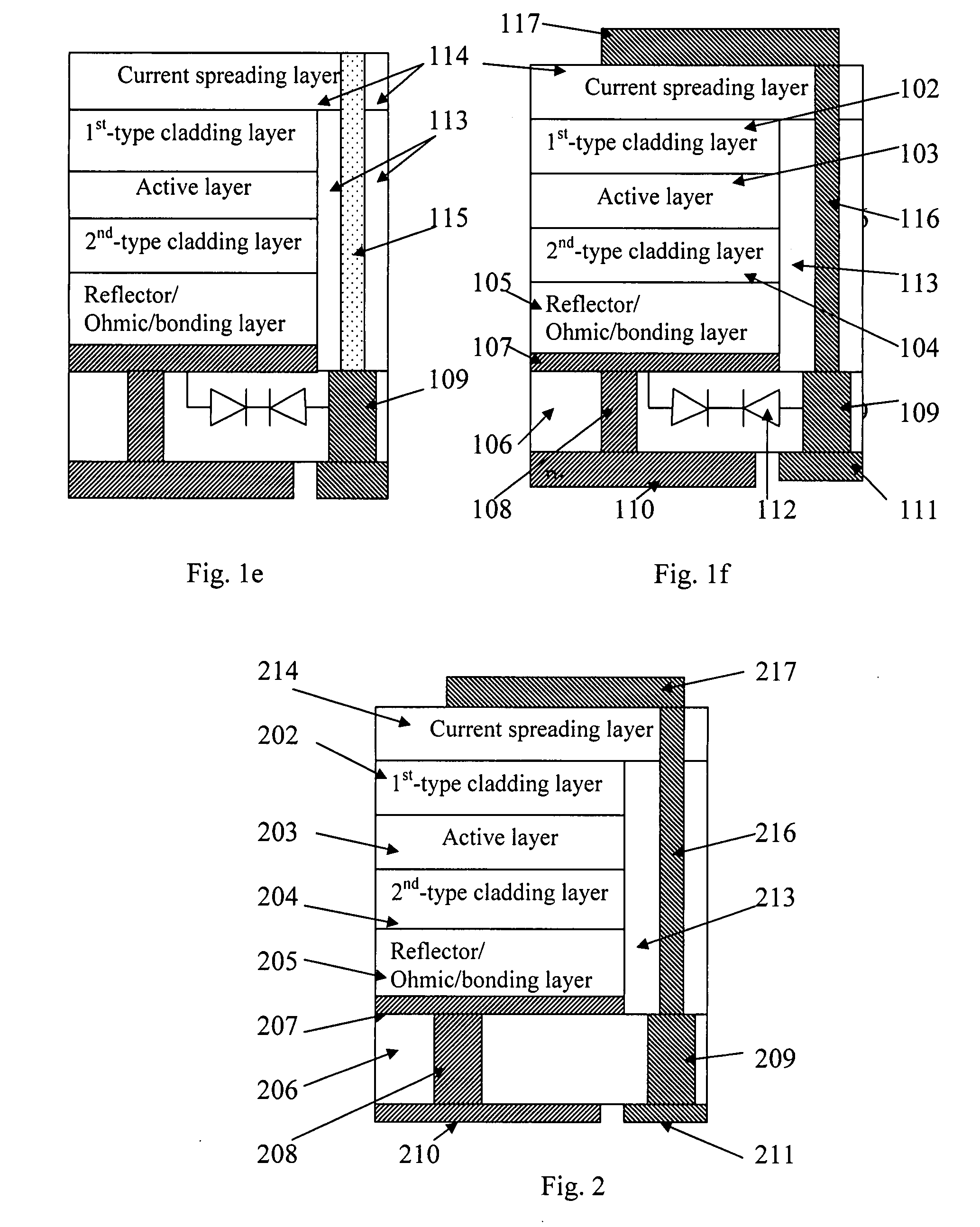
[0068]FIG. 4 shows third embodiment of through-hole vertical semiconductor devices or chips with built-in static protection diodes. Its structure and manufacturing process are substantially the same as that of FIG. 3, except that there is a current spreading layer 414 deposited on the top surfaces of both patterned electrode 417 and first-type cladding layer 402.

[0069]FIG. 5 shows second embodiment of through-hole vertical semiconductor devices or chips without built-in static protection diode. Its structure and manufacturing process are substantially the same as that of the through-hole vertical semiconductor device or chip with built-in static protection diode of FIG. 3, except that there is no built-in static protection diode in the supporting wafer. Therefore, the material of the supporting wafers is selected from a group comprising silicon, AlN, GaAs, GaP, ZnO.

[0070]FIG. 6 shows third embodiment of through-hole vertical semiconductor devices or chips without built-in static pro...


PUM


Abstract

The present invention discloses through-hole vertical semiconductor devices and chips. The structure of an embodiment of through-hole vertical semiconductor devices and chips having static protection diodes is the following: a semiconductor epitaxial layer is bonded to the first surface of a supporting chip with static protection diode; the first-type cladding layer of the semiconductor epitaxial layer is electrically connected to a first electrode on the second surface of the supporting chip via a current spreading layer, a patterned electrode, a half-through-hole-metal-plug and a through-hole-metal-plug; the second-type cladding layer of the semiconductor epitaxial layer is electrically connected to a second electrode on the second surface of the supporting chip via a reflector/Ohmic/bonding layer and at least one through-hole-metal-plug. An external power source is electrically connected to the first and second electrodes without wire bonding.

Description

BACKGROUND OF THE INVENTION[0001](1) Field of the Invention[0002]The present invention discloses through-hole vertical semiconductor devices or chips comprising through-hole vertical semiconductor GaN based, GaP based, GaNP based and ZnO based devices or chips (comprising through-hole vertical GaN based, GaP based, GaNP based and ZnO based LED) and low cost methods of manufacturing the same.[0003](2) Prior Art[0004]High power semiconductor devices or chips comprising GaN based, GaP based, GaNP based and ZnO based devices or chips (comprising GaN based, GaP based, GaNP based and ZnO based LEDs) have huge market. However, (1) technical and manufacturing issues (including heat dissipation and yield) need to be resolved; (2) performance and reliability need to be continuously improved; (3) products become smaller, thinner and lighter. In order to resolve the issues mentioned above, several methods have been disclosed, comprising: (1) vertical GaP based LED chips are disclosed to resolve...

Claims


Application Information

Patent Timeline
Patent Type & Authority Applications(United States)
IPC IPC(8): H01L33/00H01L33/48H01L33/62
CPCH01L25/167H01L33/0079H01L33/486H01L33/385H01L2924/0002H01L33/62H01L2924/00H01L33/0093
Inventor PENG, YI FANG
Owner JING PENG
Why Eureka
Try Eureka