Semiconductor device and method of forming the same

Inactive Publication Date: 2008-02-07
ELPIDA MEMORY INC
View PDF7 Cites 29 Cited by
  • Summary
  • Abstract
  • Description
  • Claims
  • Application Information

AI Technical Summary

Benefits of technology

[0016]It is another object of the present invention to provide a method of forming a semiconductor device including a capacitor with a bottom electrode with an increased adhesiveness to an adjacent insulating film.
[0017]It is still another object of the present invention to provide a method of forming a semiconductor device including a capacitor with a reduced leakage of current.
[0018]It is yet another object of the present invention to provide a method of for

Problems solved by technology

The advanced microprocessing technique has realized shrinkage of the memory cell, which decreases the charge storage capacity of a memory cell.
In recent years, further shrinkage and high density integration of a memory device such as a DRAM has caused further structural complication of a capacitor and further increase in the aspect ratio thereof.
However, the adhesive layer of titanium nitride does not ensure the adhe

Method used


Image

  • Semiconductor device and method of forming the same
  • Semiconductor device and method of forming the same
  • Semiconductor device and method of forming the same

Examples


first embodiment

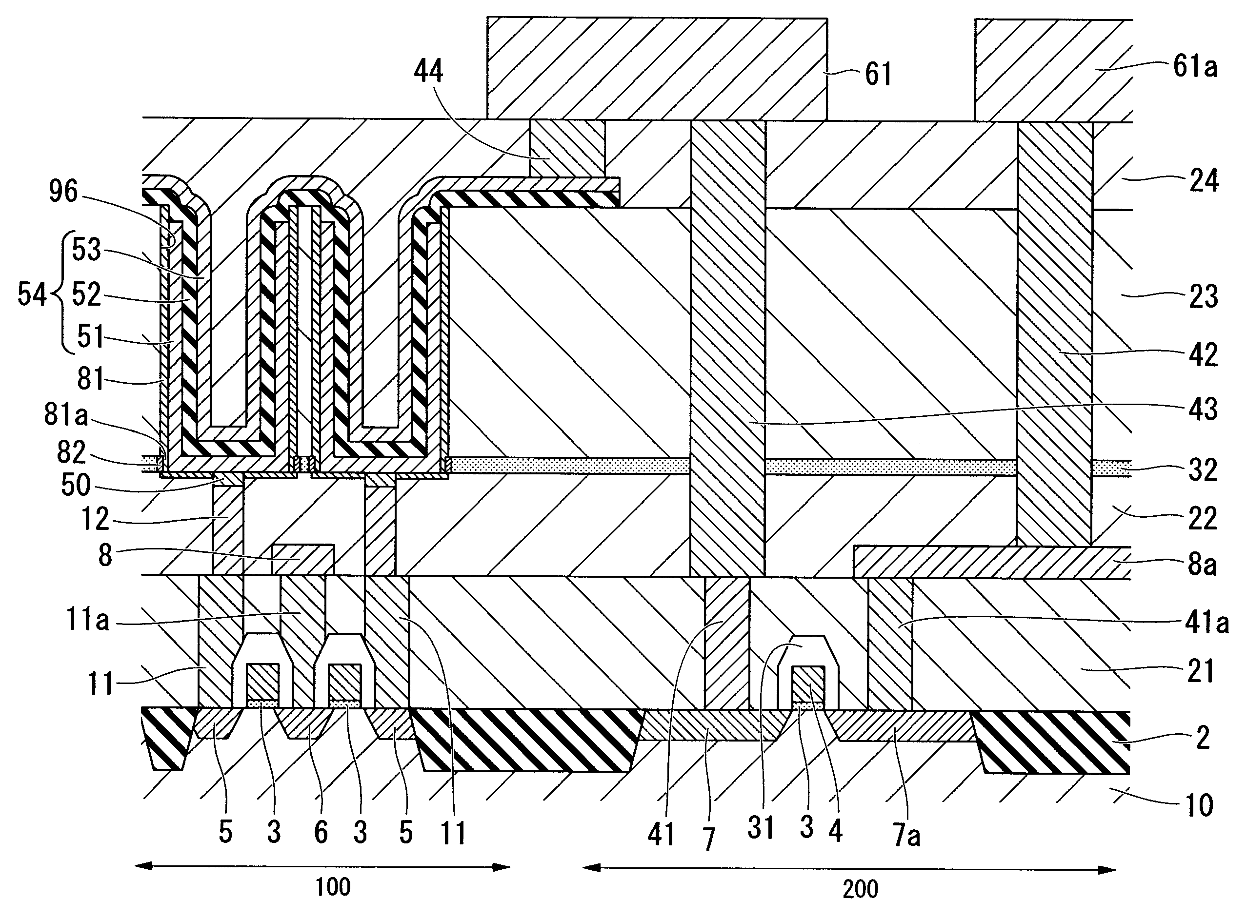
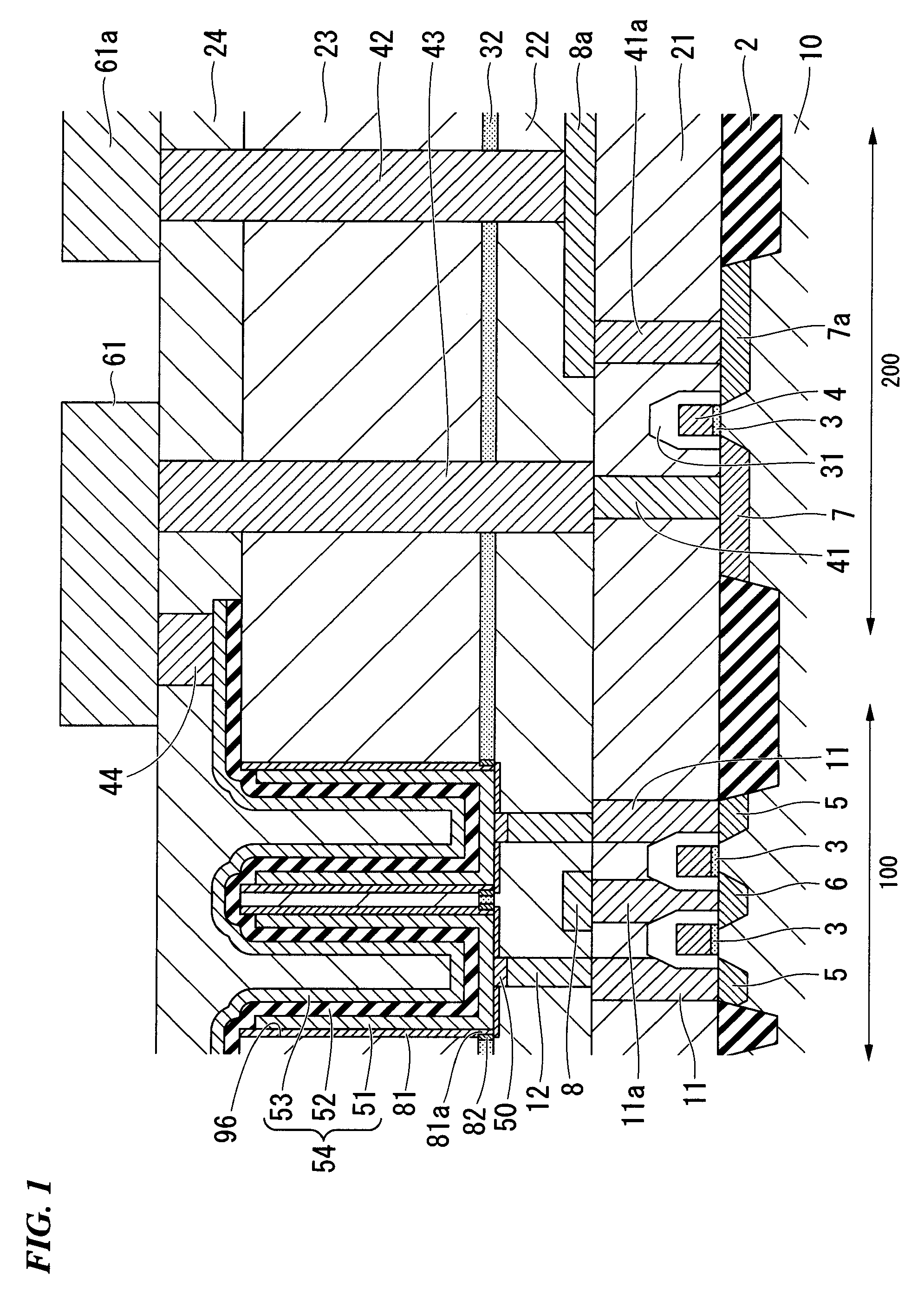
[0094]The first embodiment provides a semiconductor memory device including a metal-insulator-metal capacitor and a method of forming the same. The descriptions of the first embodiment will be made with reference to FIGS. 1-16.

(1) Semiconductor Memory Device and Capacitor Structure:

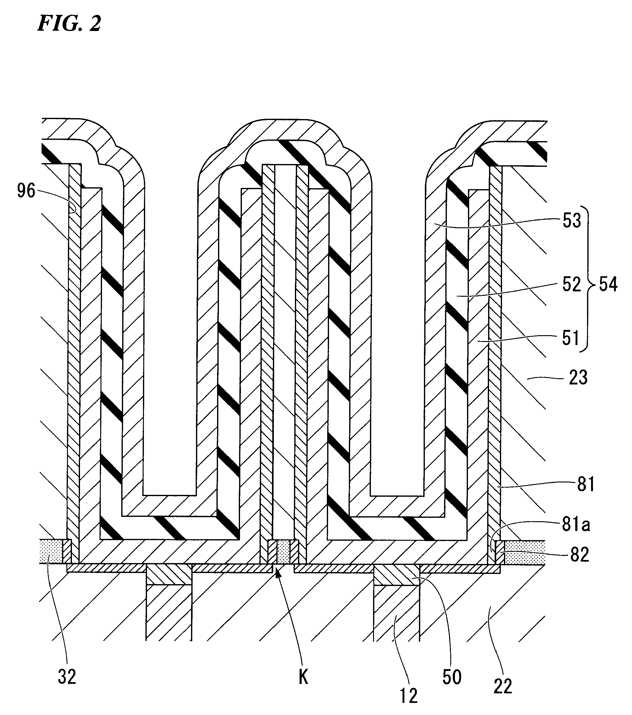
[0095]FIG. 1 is a fragmentary cross sectional elevation view illustrating a semiconductor memory device in accordance with a first preferred embodiment of the present invention. The semiconductor memory device includes a memory cell area 100 and a peripheral circuit area 200, which are adjacent to each other. The memory cell area 100 has a memory cell. The peripheral circuit area 200 has a peripheral circuit. The semiconductor memory device has a silicon substrate 10 that has a main face. An isolating film 2 such as a local oxidation of silicon film is disposed on the main face of the silicon substrate 10.

[0096]In the memory cell area 100, the isolation film 2 defines a first active region of the silicon ...

second embodiment

[0159]The second embodiment provides a semiconductor memory device including a metal-insulator-metal capacitor and a method of forming the same. The descriptions of the second embodiment will be made with reference to FIGS. 17-22.

(1) Semiconductor Memory Device and Capacitor Structure:

[0160]FIG. 17 is a fragmentary cross sectional elevation view illustrating a semiconductor memory device in accordance with a second preferred embodiment of the present invention. FIG. 18 is a fragmentary enlarged cross sectional view illustrating a capacitor structure included in a memory cell in the semiconductor device of FIG. 17.

[0161]Similarly to the first embodiment, the semiconductor memory device of the second embodiment includes the memory cell area 100 and the peripheral circuit area 200, which are adjacent to each other. The memory cell area 100 has the memory cell which includes the memory cell transistors and the capacitor 54. The peripheral circuit area 200 has the peripheral circuit.

[016...

third embodiment

[0188]The third embodiment provides a semiconductor memory device including a metal-insulator-metal capacitor including a pedestal bottom electrode and a method of forming the same. The descriptions of the third embodiment will be made with reference to FIGS. 23-29.

(1) Semiconductor Memory Device and Capacitor Structure:

[0189]FIG. 23 is a fragmentary cross sectional elevation view illustrating a semiconductor memory device in accordance with a third preferred embodiment of the present invention. FIG. 24 is a fragmentary enlarged cross sectional view illustrating a capacitor structure with a pedestal bottom electrode which is included in a memory cell in the semiconductor device of FIG. 23.

[0190]Similarly to the first embodiment, the semiconductor memory device of the second embodiment includes the memory cell area 100 and the peripheral circuit area 200, which are adjacent to each other. The memory cell area 100 has the memory cell which includes the memory cell transistors and the ...


PUM


Abstract

A semiconductor device includes a first insulating layer, a capacitor, an adhesive layer, and an intermediate layer. The first insulating layer may include a first insulating film. The first insulating layered structure has a first hole. The capacitor is disposed in the first hole. The capacitor may include bottom and top electrodes and a capacitive insulating film. The capacitive insulating film is sandwiched between the bottom and top electrodes. The adhesive layer contacts with the bottom electrode. The adhesive layer has adhesiveness to the bottom electrode. The intermediate layer is interposed between the adhesive layer and the first insulating film. The intermediate layer contacts with the adhesive layer and with the first insulating film. The intermediate layer has adhesiveness to the adhesive layer and to the first insulating film.

Description

BACKGROUND OF THE INVENTION[0001]1. Field of the Invention[0002]The present invention generally relates to a semiconductor device and a method of forming the same. More specifically, the present invention relates to a semiconductor device including a DRAM capacitor with a bottom electrode having an improved adhesiveness with an adjacent insulating film.[0003]Priority is claimed on Japanese Patent Application No. 2006-211168, filed Aug. 2, 2006, the content of which is incorporated herein by reference.[0004]2. Description of the Related Art[0005]All patents, patent applications, patent publications, scientific articles, and the like, which will hereinafter be cited or identified in the present application, will hereby be incorporated by reference in their entirety in order to describe more fully the state of the art to which the present invention pertains.[0006]A memory cell such as a DRAM (Dynamic Random Access Memory) includes a switching transistor and a capacitor. The advanced mi...

Claims


Application Information

Patent Timeline
IPC IPC(8): H01L27/108H01L21/336
CPCH01L27/10852H01L28/91H01L27/10894H10B12/033H10B12/09
Inventor NAKAMURA, YOSHITAKA
Owner ELPIDA MEMORY INC
Why Eureka
Try Eureka