Conductive shielding pattern and semiconductor structure with inductor device

a technology of inductor device and shielding pattern, which is applied in the direction of semiconductor device, semiconductor/solid-state device details, electrical apparatus, etc., can solve the problems of eddy current within the conductive layer obstructing and counteracting, and the quality of the inductor device is lower, so as to improve the quality and the factor q of the inductor device

Inactive Publication Date: 2008-02-07
UNITED MICROELECTRONICS CORP
View PDF8 Cites 17 Cited by
  • Summary
  • Abstract
  • Description
  • Claims
  • Application Information

AI Technical Summary

Benefits of technology

[0013]Accordingly, at least one objective of the present invention is to provide a conductive shielding pattern capable of improving the quality and the factor Q of the inductor device.
[0030]In the present invention, since the alternative arrangement of the conductive layers and the diffusion regions is the conductive shielding pattern for shielding the inductor device, the permeance interference of the substrate to the inductor device is decreased and the performance of the chip is increased. Meanwhile, the eddy current is hardly generated by the novel conductive shielding pattern so that the inductance of the inductor device is maintained and the parasitic capacitance is decreased.

Problems solved by technology

Since the inductor device is located close to the silicon substrate, the silicon substrate turns to be a conductor to consume a large amount of energy to lower the quality of the inductor device under the high frequency of the high frequency device.
Accordingly, when the conductive layer is really close to the inductor device, the eddy current within the conductive layer would obstruct and counteract the magnetic field generated by the spiral inductor device.

Method used


Image

  • Conductive shielding pattern and semiconductor structure with inductor device
  • Conductive shielding pattern and semiconductor structure with inductor device
  • Conductive shielding pattern and semiconductor structure with inductor device

Examples


Embodiment Construction

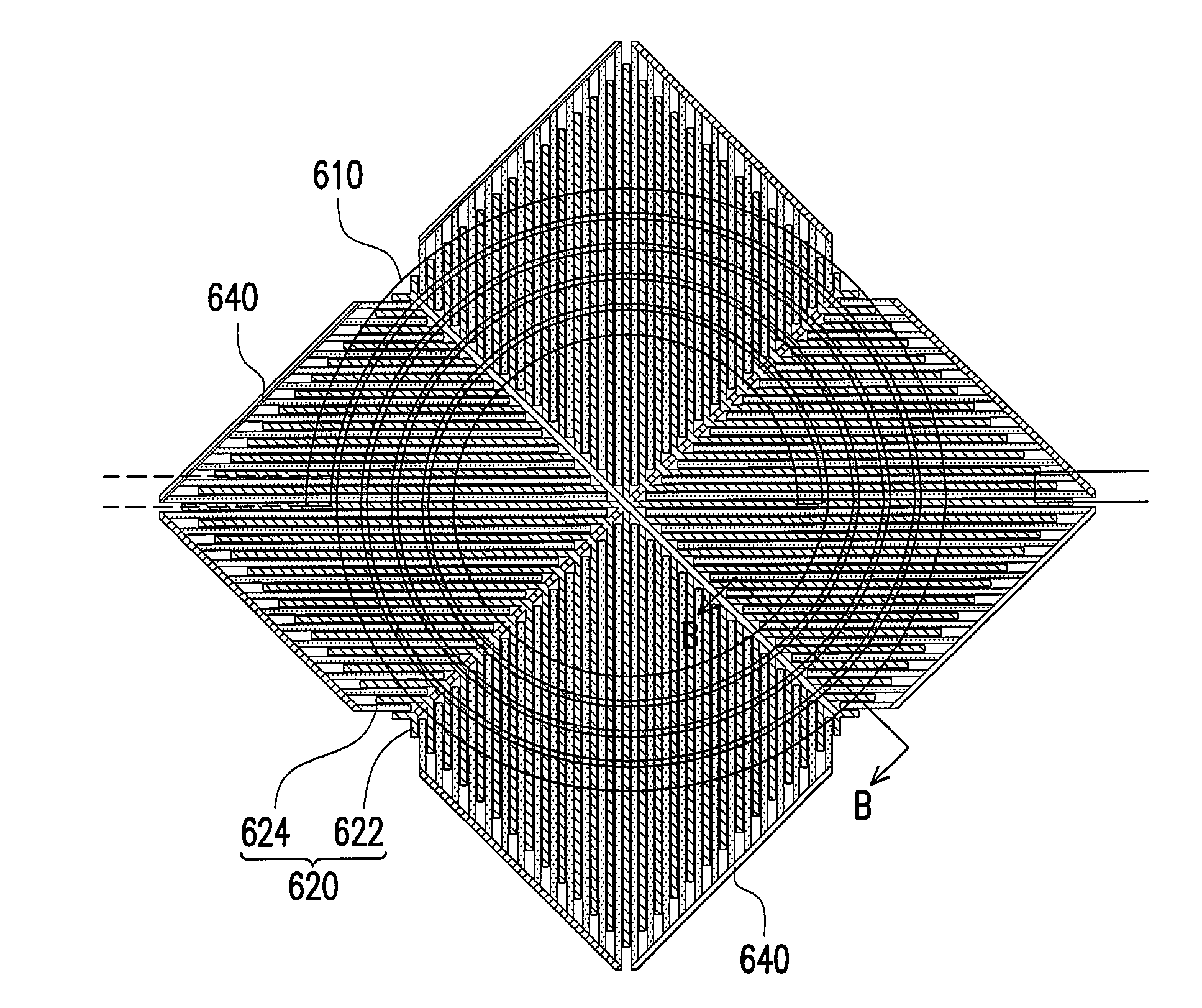
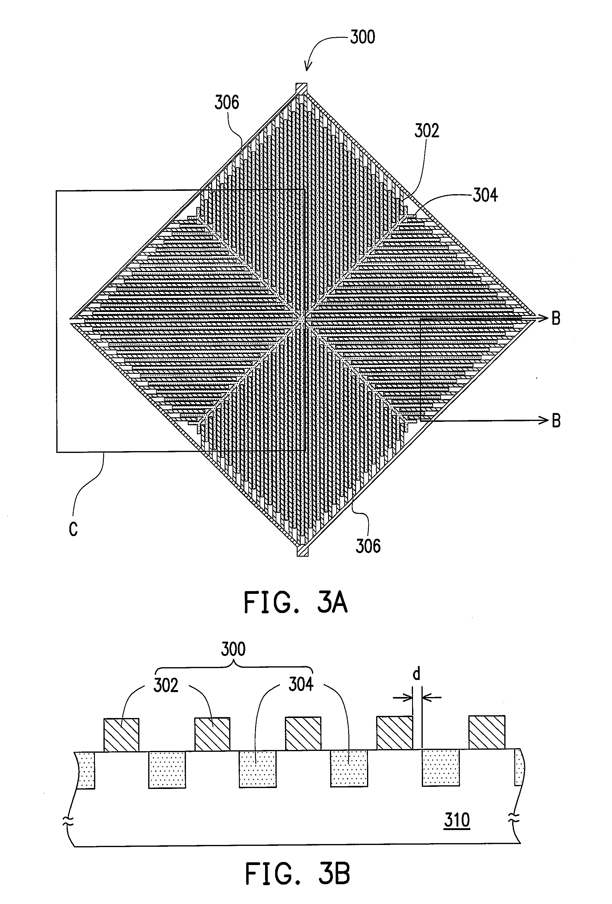
[0043]FIG. 3A is a top view showing a conductive shielding pattern according to one embodiment of the present invention. FIG. 3B is a cross-sectional view of FIG. 3A along line B-B. FIG. 3C is an enlarged diagram of a C region of FIG. 3A.

[0044]As shown in FIG. 3A together with FIGS. 3B and 3C, in this embodiment, the conductive shielding pattern 300 is used to shield an inductor device (not shown). This conductive shielding pattern 300 is composed of alternatively arranged conductive layers 302 and diffusion regions 304. The conductive layers are made of polysilicon or metal such as copper, gold, nickel, aluminum and tungsten. The conductive layers 302 are located on the substrate 310 and the diffusion regions 304 are located in the substrate 310. The conductive layers 302 and the diffusion regions 304 are free ends. Moreover, the conductive shielding pattern 300 of this embodiment further comprises several metal lines 306 located conductive layers 302 and the diffusion regions 304 ...


PUM


Abstract

The invention is directed to a conductive shielding pattern for shielding a inductor device. The conductive shielding pattern comprises a plurality of conductive layers and a plurality of diffusion regions. The conductive layers are located on a substrate. The diffusion regions are located in the substrate and the conductive layers and the diffusion regions are arranged alternatively and are free ends respectively.

Description

BACKGROUND OF THE INVENTION[0001]1. Field of Invention[0002]The present invention relates to a semiconductor device. More particularly, the present invention relates to a conductive shielding pattern and a semiconductor device having an inductor device.[0003]2. Description of Related Art[0004]In the integrated circuit, the inductor device is an importance device. Generally, the inductor device is a round shape or square shape spiral metal coil. Moreover, the inductor device can be widely used. For the high frequency application field, it demands relatively high quality of the inductor device. That is, the inductor device possesses relatively high quality factor Q in this application field. The factor Q mentioned above is defined according to:Q=ω0×L / R (1), wherein ω0 indicates the resonant angular frequency of the inductor device, R indicates the resistance of the inductor device and L indicates the inductance of the metal coil. Since the inductor device is located close to the silic...

Claims


Application Information

Patent Timeline
Patent Type & Authority Applications(United States)
IPC IPC(8): H01L23/552
CPCH01L23/5225H01L27/08H01L23/5227H01L2924/0002
Inventor HUNG, CHENG-CHOUTSENG, HUA-CHOUCHEN, YU-CHIALIANG, VICTOR-CHIANGFAN, CHENG-WEN
Owner UNITED MICROELECTRONICS CORP
Why Eureka
Try Eureka