Structure and method of making lidded chips

a technology of lidded chips and chips, which is applied in the field of microelectronic packaging, can solve the problems of requiring a relatively complex series of steps for the formation of terminals on the caps and vias for connecting the terminals to the contacts on the active wafer, and requiring the provision of terminals for mems devices

Inactive Publication Date: 2008-02-07
TESSERA INC
View PDF99 Cites 101 Cited by
  • Summary
  • Abstract
  • Description
  • Claims
  • Application Information

AI Technical Summary

Benefits of technology

[0048] Desirably, the mechanical strength of the lidded chip is increased by presence of the heat spreader.
[0071] In one embodiment, the metal foil functions as an electromagnetic screen to prevent passage of electromagnetic radiation at frequencies of interest.
[0073] In accordance with another aspect of the invention, a lidded optoelectronic device chip is provided which includes a chip having an optoelectronic device. Desirably, microelectronic circuits are exposed at a surface of the chip. A lid may be mounted to overlie the optoelectronic device and the microelectronic circuits of the chip. A plurality of light polarizing filters having different polarizations may be mounted to either the chip or the lid. At least two of the plurality of light polarizing filters can have different polarizations. The filters may cover the same area overlying the microelectronic circuits and may block at least some light from reaching the microelectronic circuits.
[0076] In a particular embodiment, the metal foil can function as an electromagnetic screen to prevent passage of electromagnetic radiation at frequencies of interest.

Problems solved by technology

This increases the area of the active wafer required to form each unit, requires additional operations and results in an assembly considerably larger than the unit itself.
However, formation of terminals on the caps and vias for connecting the terminals to the contacts on the active wafer requires a relatively complex series of steps.
Similar problems occur in providing terminals for MEMS devices.

Method used


Image

  • Structure and method of making lidded chips
  • Structure and method of making lidded chips
  • Structure and method of making lidded chips

Examples


Embodiment Construction

[0181] Particular types of devices, such as SAW devices and MEMs need to be sealed hermetically in order to function appropriately over the life of the device. For many silicon semiconductor devices, a package is considered to be hermitic if it has a leak rate of helium below 1×10⁻⁸ Pa m3 / sec. Other devices such as electro-optical devices do not require hermeticity, but nevertheless are best packaged under a protective lid, e.g., one that is optically transmissive, as a way of preventing particles from reaching a surface of the electro-optic device.

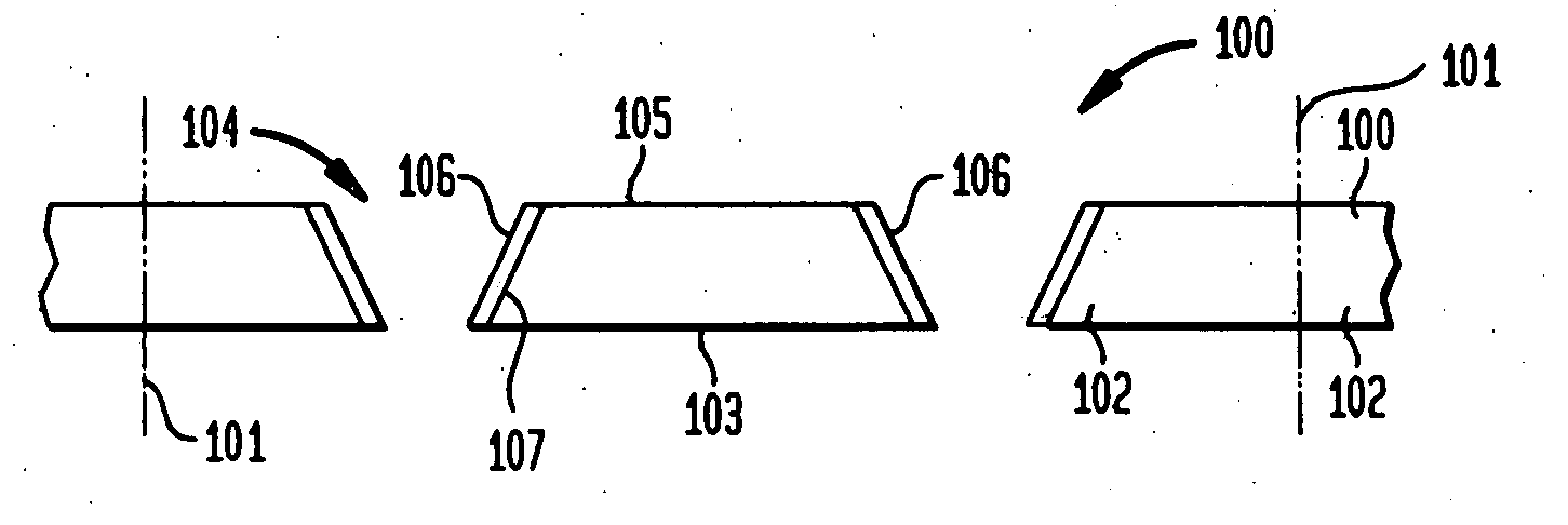
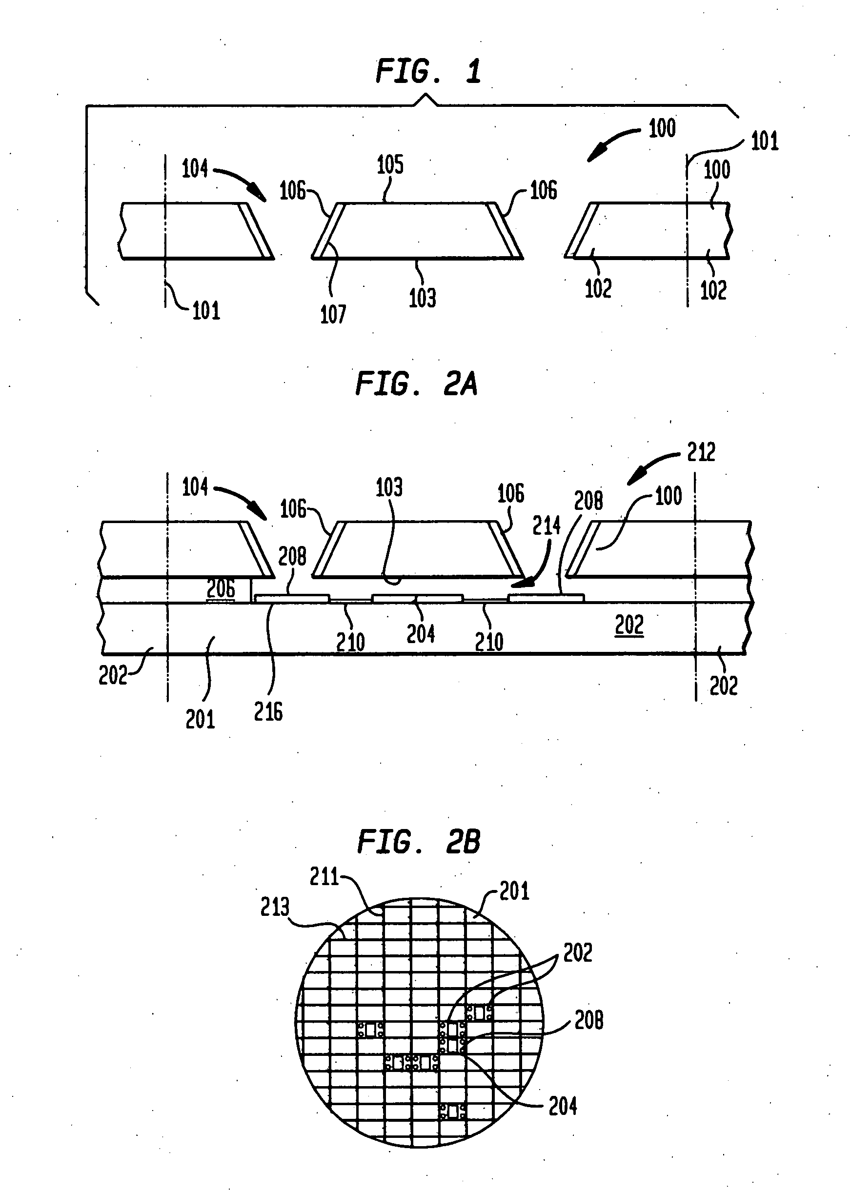
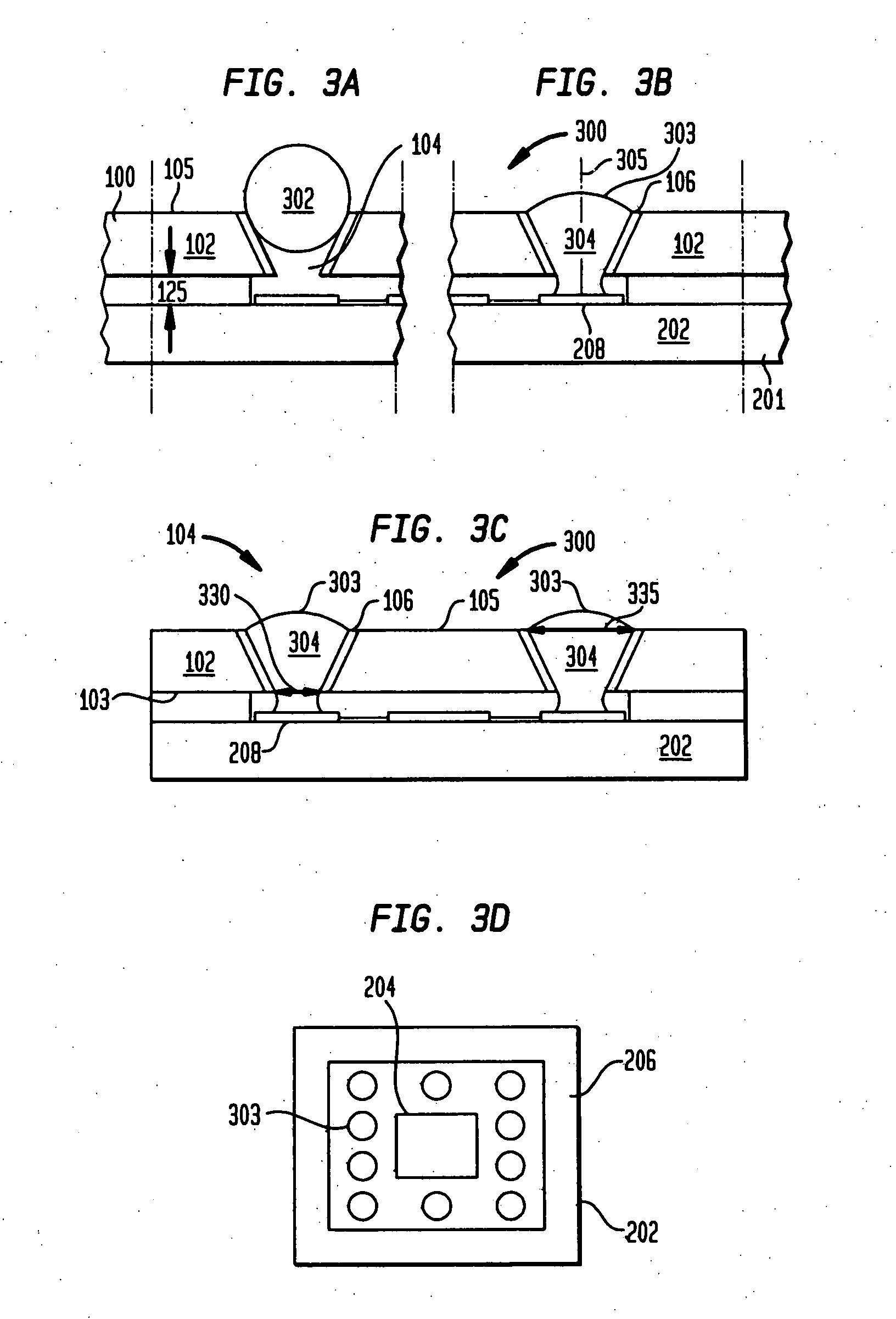
[0182] With reference to FIGS. 1-3D, in a method of forming the capped chips, a plurality of caps 102, e.g., as contained in a multiple cap-containing element 100 or wafer, are simultaneously mounted to a plurality of chips, e.g., a wafer containing the chips, and then the chips are severed to form capped chip units 300, as best seen in FIG. 3C. In such method, as shown in FIG. 1, the cap element 100 includes a plurality of caps 102, joi...


PUM

PropertyMeasurementUnit
temperaturesaaaaaaaaaa
thicknessaaaaaaaaaa
pore heightaaaaaaaaaa

Abstract

Lidded chip packages are provided in which an optoelectronic device chip has microelectronic circuits exposed at a surface of the chip with a lid mounted to overlie the optoelectronic device and the microelectronic circuits. An opaque film may be attached to the lid to overlie the microelectronic circuits while exposing the optoelectronic device. Lidded chip packages are also provided in which the lid overlies an active or passive device mounted to the chip. Wiring traces may be embedded within an adhesive between the lid and the chip.

Description

CROSS-REFERENCE TO RELATED APPLICATIONS [0001] This application claims the benefit of the filing date of U.S. Provisional Patent Application No. 60 / 777,940 filed Mar. 1, 2006, the disclosure of which is hereby incorporated herein by reference. The following applications are hereby incorporated by reference herein. U.S. patent application Ser. No. 10 / 949,575 filed Sep. 24, 2004, U.S. Provisional Patent Application Nos. 60 / 506,500 filed Sep. 26, 2003 60 / 515,615 filed Oct. 29, 2003, 60 / 532,341 filed Dec. 23, 2003, 60 / 568,041 filed May 4, 2004, 60 / 574,523 filed May 26, 2004, and U.S. patent application Ser. No. 10 / 928,839 filed Aug. 27, 2004. The following U.S. patent applications and U.S. Provisional patent applications are also hereby incorporated herein by reference: Ser. Nos. 11 / 121,434 filed May 4, 2005, 10 / 711,945 filed Oct. 14, 2004, 11 / 120,711 filed May 3, 2005, 11 / 068,830 filed Mar. 1, 2005, 11 / 068,831 filed Mar. 1, 2005, 11 / 016,034 filed Dec. 17, 2004, 11 / 284,289 filed Nov. 21...

Claims


Application Information

Patent Timeline
Patent Type & Authority Applications(United States)
IPC IPC(8): H01L23/10H01L21/58
CPCB81B2207/095H01L2924/10253B81C2203/0118C04B2237/366H01L27/14618H01L31/0203H01L2224/32225H01L2224/48227H01L2224/4824H01L2224/73265H01L2924/15311B81C1/00301H01L2924/07811H01L2924/3025H01L2924/3011H01L2224/11334H01L2924/1461H01L2924/01322H01L2924/01327H01L2224/8592H01L2224/48091H01L2924/00014H01L2924/00H01L2224/05573H01L2224/05568H01L2224/056H01L2224/06135H01L24/05
Inventor TUCKERMAN, DAVID B.HUMPSTON, GILESNYSTROM, MICHAEL J.BEROZ, MASUDTHOMPSON, JESSE BURL
Owner TESSERA INC
Why Eureka
Try Eureka