Semiconductor memory device having a plurality of chips and capability of outputting a busy signal
a memory device and semiconductor technology, applied in the field of semiconductor memory devices, can solve the problems of increasing the manufacturing cost of memory chips, the inability to control the memory chips from the outside, and the possibility of manufacturing defective memory cells high
- Summary
- Abstract
- Description
- Claims
- Application Information
AI Technical Summary
Benefits of technology
Problems solved by technology
Method used
Image
Examples
first embodiment
[0090]FIG. 8 is a circuit diagram specifically showing a partial configuration of the busy control circuit 32 in FIG. 4 which is provided in each of the two memory chips MC1 and MC2 in the memory device according to the present invention. In this case, the above-mentioned method (2) is used.
[0091] The busy control circuit 32 has the same circuit configuration in both memory chips MC1 and MC2. The busy control circuits are represented by the reference numerals 32-1 and 32-2 in the memory chips MC1 and MC2, respectively.
[0092] At the power-on time, the memory chips MC1 and MC2 generate internal busy signals busy1 and busy2. Each of busy signals busy1 and busy2 is supplied to the gate of an N-channel MOS transistor 51 and one input terminal of a 2-input NOR circuit 52 in the busy control circuits 32-1 and 32-2. The source of the transistor 51 is connected to the ground voltage node. The drain is connected to the busy state output terminal 11 via the pad on the chip. As mentioned above...
second embodiment
[0114]FIG. 13 is a circuit diagram specifically showing a partial configuration of the busy control circuit 32 in the memory device according to the present invention. In this case, the above-mentioned method (1) is used.
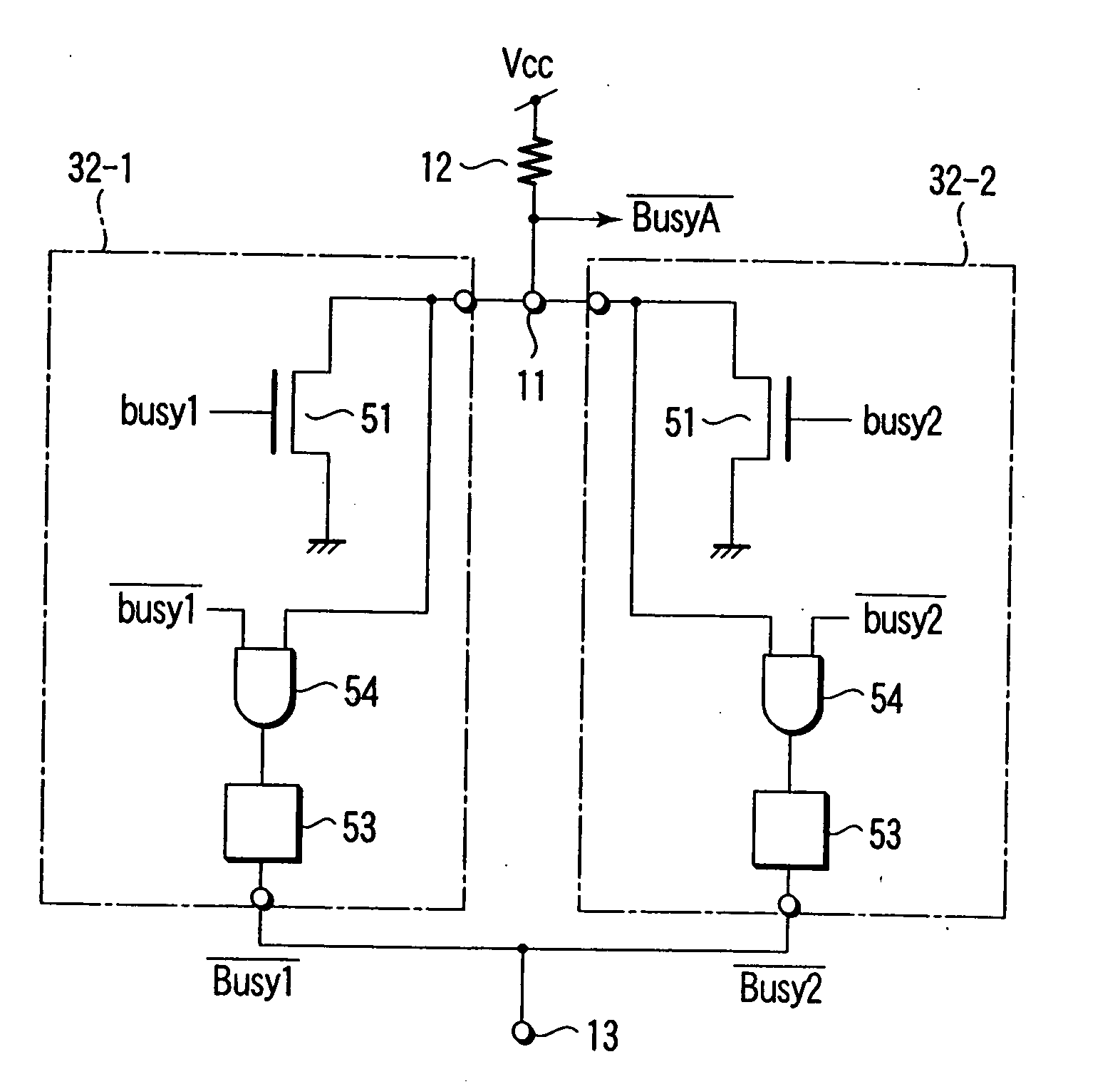
[0115] The busy control circuit 32 has the same circuit configuration in both memory chips MC1 and MC2. The busy control circuits are represented by the reference numerals 32-1 and 32-2 in the memory chips MC1 and MC2, respectively. The busy control circuits 32-1 and 32-2 each are provided with the N-channel MOS transistor 51, the output control circuit 53, and the 2-input AND circuit 54. The gate of the MOS transistor 51 is supplied with internal busy signals busy1 and busy2 generated in the memory chips MC1 and MC2. The source of the transistor 51 is connected to the ground voltage node. The drain is connected to the busy state output terminal 11 via the busy state output pad on the chip. The terminal 11 is connected to the node of the power supply voltage Vcc via...
third embodiment
[0120]FIG. 14 is a circuit diagram specifically showing a partial configuration of the busy control circuit 32 in the memory device according to the present invention. In this case, the above-mentioned method (2) is used.
[0121] The busy control circuit 32 has the same circuit configuration in both memory chips MC1 and MC2. The busy control circuits are represented by the reference numerals 32-1 and 32-2 in the memory chips MC1 and MC2, respectively.
[0122] The busy control circuits 32-1 and 32-2 each are provided with the N-channel MOS transistor 51, the output control circuit 53, the 2-input AND circuit 55, an N-channel MOS transistor 56, and a load resistor 57. The gate of the MOS transistor 51 is supplied with internal busy signals busy1 and busy2 generated in the memory chips MC1 and MC2. The source of the transistor 51 is connected to the ground voltage node. The drain is connected to the busy state output terminal 11 via the busy state output pad on the chip. The terminal 11 i...
PUM
 Abstract
Description
Claims
Application Information


