Pseudo-differential analog front end circuit and image processing device

a front end circuit and pseudodifferential technology, applied in the field of display systems, can solve problems such as signal distortion, achieve the effects of reducing the number of components, reducing power consumption and the size of analog circuits, and improving the quality characteristic of input buffers

Active Publication Date: 2008-02-14
REALTEK SEMICON CORP
View PDF5 Cites 6 Cited by
  • Summary
  • Abstract
  • Description
  • Claims
  • Application Information

AI Technical Summary

Benefits of technology

[0011]A feature of the invention is that each of the ADCs receives a common comparing voltage circuit to form the pseudo-differential AFE circuit. The term “pseudo-differential AFE circuit” refers to front-end circuits connected respectively to the positive input terminal and the negative input terminal of the ADC. In fact, the front-end circuits have pseudo symmetric circuit configuration instead of a fully differential input structure. The invention makes use of the least components and the least number of pins to form the pseudo-differential AFE circuit so as to approximate to an AFE circuit with fully-differential inputs. The invention solves both the signal distortion problem caused by a singled-ended to differential conversion and drawbacks of the AFE circuit with fully-differential inputs, such as having too many components and too many package pins. Therefore, the invention not only reduces the number of components and the number of package pins in the peripheral circuit and the AFE circuit to reduce the power consumption and the size of the analog circuit, but also improves the quality characteristic of the input buffer based on a pseudo-differential input structure, thereby rendering a much better image quality.

Problems solved by technology

However, converting singled-ended signals into differential signals may cause a signal distortion problem due to different reference ground levels.

Method used


Image

  • Pseudo-differential analog front end circuit and image processing device
  • Pseudo-differential analog front end circuit and image processing device
  • Pseudo-differential analog front end circuit and image processing device

Examples


first embodiment

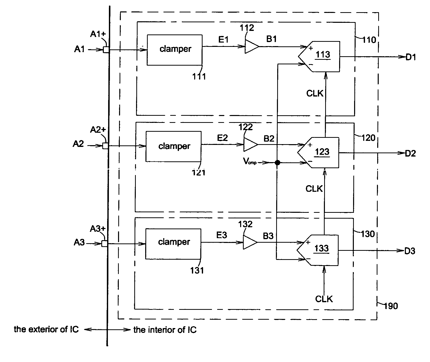
[0024]It should be noted that, in the first embodiment, the negative input terminals of the three ADCs 113, 123, 133 can be also referenced to the internal ground (inside the IC) that is shared by three channels A1, A2, A3 (not shown), thereby replacing the architecture having an additional pin A2− (shown in FIG. 2) connected to an external ground (outside the IC) and maintaining the same image quality. This is because the common-mode noise between the positive input terminal and the negative input terminal can be counteracted by means of the use of the pseudo-differential input structure, accordingly saving the pin A2−.

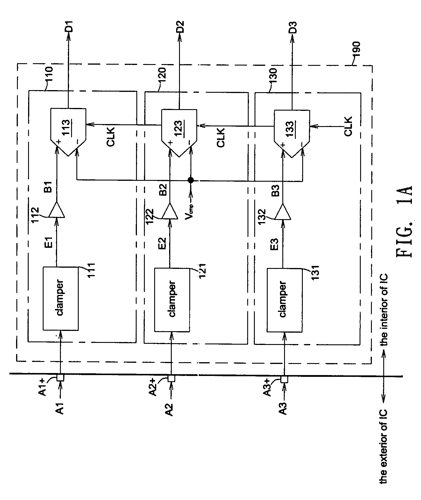
[0025]FIG. 3 shows a schematic circuit diagram of an image processing device according to a second embodiment of the invention. Referring to FIG. 3, an image processing device 300 of the invention, including a peripheral circuit 380 and a pseudo-differential AFE circuit 390, receives and processes analog image signals A1, A2, A3 from a display card 170 to generate di...

second embodiment

[0026]It should be noted that, in the second embodiment, the negative input terminals of the three ADCs 113, 123, 133 can be also referenced to the internal ground (inside the IC) that is shared by three channels A1, A2, A3 (not shown), thereby replacing the architecture having an additional pin A2− (shown in FIG. 3) connected to an external ground (outside the IC) and maintaining the same image quality. This is because the common-mode noise between the positive input terminal and the negative input terminal can be counteracted by means of the use of the pseudo-differential input structure, accordingly saving the pin A2−.

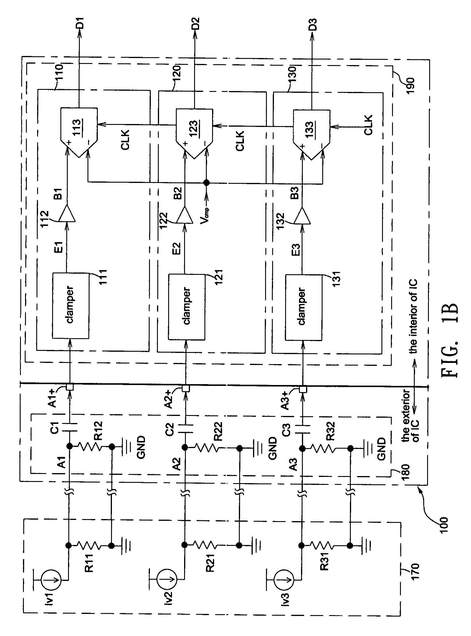
[0027]FIG. 4 shows a schematic circuit diagram of an input buffer according to the invention. According to the invention, based on the feature of the pseudo-differential input structure and a constant voltage difference between the positive input terminal and the negative input terminal, voltage levels at the positive input terminals and the negative input terminals...


PUM


Abstract

An image processing device is provided which includes a pseudo differential analog front end circuit for receiving at least one image analog signal and generating at least one digital signal. The pseudo differential analog front end circuit includes at least a converting circuit, each of which includes a clamper, an input buffer and an analog-to-digital converter. All of the analog-to-digital converters receive a common comparing voltage if the number of the converting circuits is greater than one.

Description

BACKGROUND OF THE INVENTION[0001]1. Field of the Invention[0002]The invention relates to display systems, and more particularly, to an image processing device applied to display systems. More specifically, the invention relates to an image processing device having a pseudo-differential analog front end circuit.[0003]2. Description of the Related Art[0004]Many display cards (e.g., VGA card) in computer systems outputs only analog image signals in an analog format, so a liquid crystal display (LCD) is capable of displaying image frames after the analog image signal is converted into a digital image signal. Usually, the liquid crystal display utilizes an analog front end (AFE) circuit to perform signal conversion. Since the analog image signals contain three signals R, G, B, the AFE circuit includes three circuits to process the three signals respectively. A liquid crystal display controller mainly includes the AFE circuit, a scalar and a peripheral circuit. As chip integration increas...

Claims


Application Information

Patent Timeline
Patent Type & Authority Applications(United States)
IPC IPC(8): H03M1/12
CPCG09G5/006
Inventor TSAI, JUI-YUAN
Owner REALTEK SEMICON CORP
Why Eureka
Try Eureka