

Systems and methods for manufacturing wire grid polarizers
- Summary
- Abstract
- Description
- Claims
- Application Information
AI Technical Summary
Benefits of technology
Problems solved by technology
Method used
Image

Examples
first embodiment
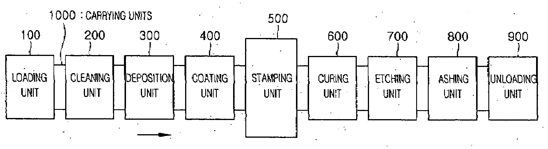
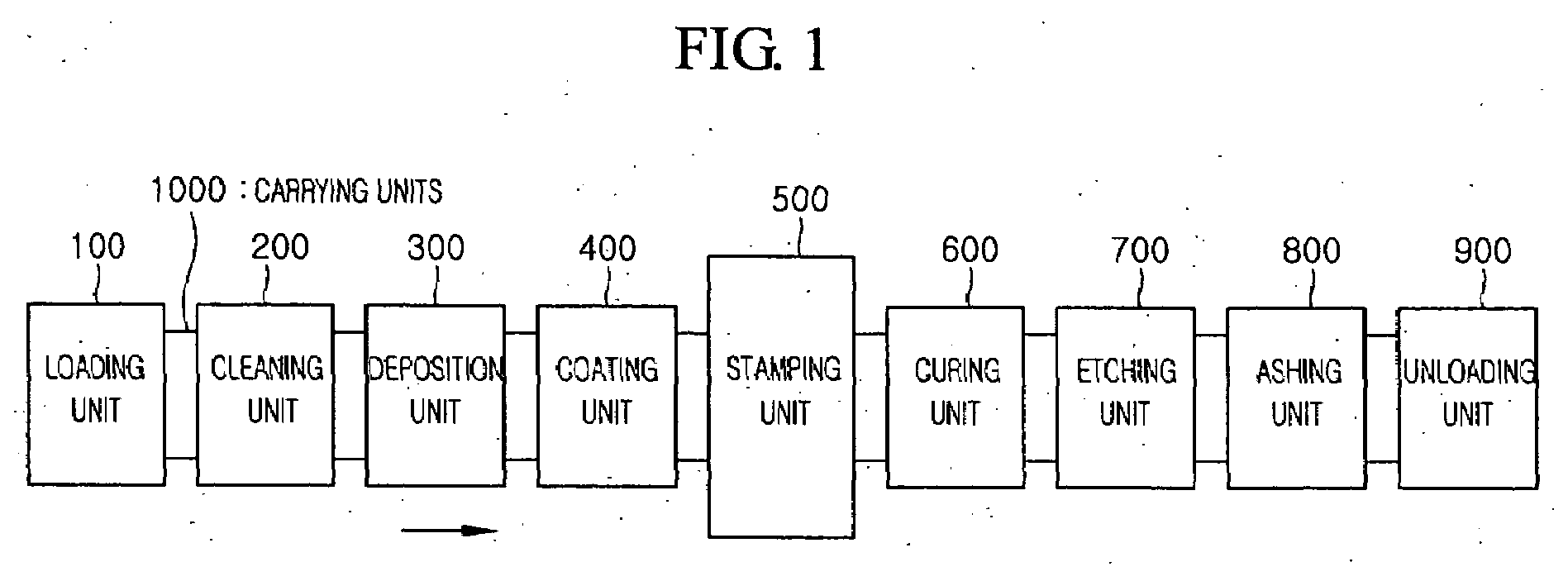
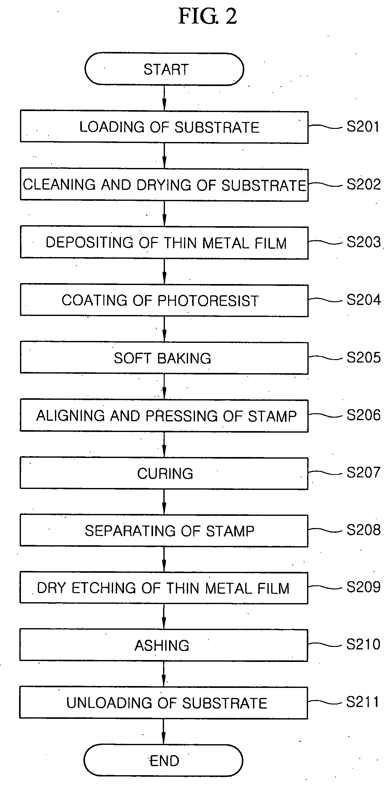
[0054]FIG. 4 is a schematic elevation view of a first exemplary embodiment of stamping and curing units 500 and 600 of an exemplary manufacturing system, and FIG. 5 is a process flow diagram of the processes carried out in stamping and curing units of FIG. 4.
[0055]Referring to FIG. 4, the stamping unit 500 includes a stamping chamber 510, a first substrate supporting unit 520 and a pressing unit 540, while the curing unit 600 includes a curing chamber 610, a second substrate supporting unit 620, and a curing source unit 630.
[0056]The stamping chamber 510 of the stamping unit 500 provides a space in which various components of the unit are installed. The first substrate supporting unit 520 is disposed in the stamping chamber 510 and serves to support a substrate 2000 carried into the stamping chamber 510. In this particular embodiment, the substrate 200 refers to a substrate on which a thin metal film layer and a photoresist have previously been sequentially formed through the unit p...
second embodiment
[0066]FIGS. 6A and 6B are a schematic elevation view and a block diagram, respectively, of a second exemplary embodiment of stamping and curing units 500 and 600 of an exemplary manufacturing system, and FIG. 7 is a process flow diagram of the processes carried out in stamping and curing units of FIGS. 6A and 6B.
[0067]The second embodiment of FIGS. 6A to 7 is different from the first exemplary embodiment of FIGS. 4 and 5 above in that a plurality of stamps is used, but except for that, is otherwise similar. The following discussion therefore focuses mainly on the differences between the two embodiments.
[0068]Referring to FIGS. 6A and 6B, the stamping unit 500 of the second embodiment includes a stamping chamber 510, a first substrate supporting unit 520, a stamp 530, a pressing unit 540 and a stamp storing chamber 550, and the curing unit 600 includes a curing chamber 610, a second substrate supporting unit 620, and a curing source unit 630.
[0069]The stamping chamber 510 of the stam...
third embodiment
[0078]Referring to FIG. 8, the stamping unit 500 of the third embodiment includes a stamping chamber 510, a first substrate supporting unit 520, a stamp 530, a pressing unit 540 and a UV light source 560, while the curing unit 600 includes a curing chamber 610, a second substrate supporting unit 620 and a heater 635.
[0079]The photoresist that is applied to the substrate in the coating unit 400 (see FIG. 1) situated upstream of the stamping unit 500 can comprise a “hybrid” photoresist, i.e., one in which a UV-curable photoresist and a thermosetting photoresist are mixed. In such a case, the UV-curable photoresist can include, for example, an acrylate polymer, and the thermosetting photoresist can include, for example, an epoxy polymer.
[0080]In light of the foregoing, the stamping unit 500 of the third embodiment of FIGS. 8 and 9 is additionally provided with the UV light source 560 for curing the UV-curable portion of the hybrid photoresist mixture. The UV light source 560 can be pro...
PUM
| Property | Measurement | Unit |
|---|---|---|
| Pressure | aaaaa | aaaaa |
| Polarity | aaaaa | aaaaa |
| Solubility (mass) | aaaaa | aaaaa |
Abstract
Description
Claims
Application Information