Physical quantity detection device, method of driving physical quantity detection device, and imaging apparatus

a technology of physical quantity and detection device, which is applied in the direction of radiation controlled devices, optical radiation measurement, semiconductor/solid-state device details, etc., can solve the problem of low signal transfer efficiency between chips, and achieve the effect of low power consumption, high speed and low power consumption

Inactive Publication Date: 2008-02-21
SONY CORP
View PDF8 Cites 160 Cited by
  • Summary
  • Abstract
  • Description
  • Claims
  • Application Information

AI Technical Summary

Benefits of technology

[0011]By the present invention, the parallel-to-serial conversion of the pixel signal is performed by the other of the semiconductor substrates, which receives a pixel signal from one of the semiconductor substrates by parallel transmission. Thus, for example when a signal processing circuit (DSP circuit) is mounted on the other of the semiconductor substrates, it is possible to serialize the pixel signal on the other of the semiconductor substrates to input the signal into the signal processing circuit while exchanging the signal at a high...

Problems solved by technology

However, in a system in which a plurality of chips are linked as the above-described known e...

Method used


Image

  • Physical quantity detection device, method of driving physical quantity detection device, and imaging apparatus
  • Physical quantity detection device, method of driving physical quantity detection device, and imaging apparatus
  • Physical quantity detection device, method of driving physical quantity detection device, and imaging apparatus

Examples


first embodiment

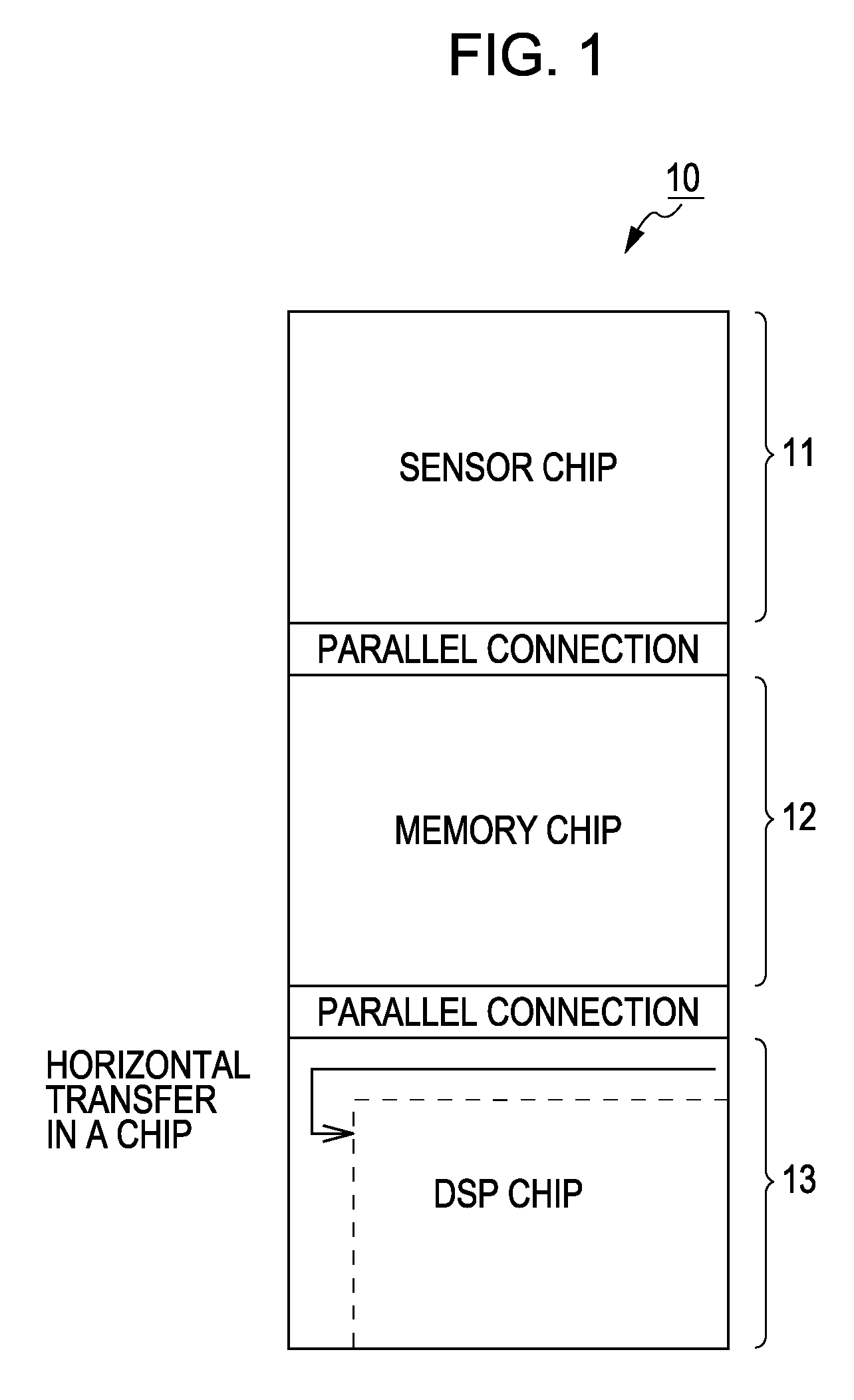
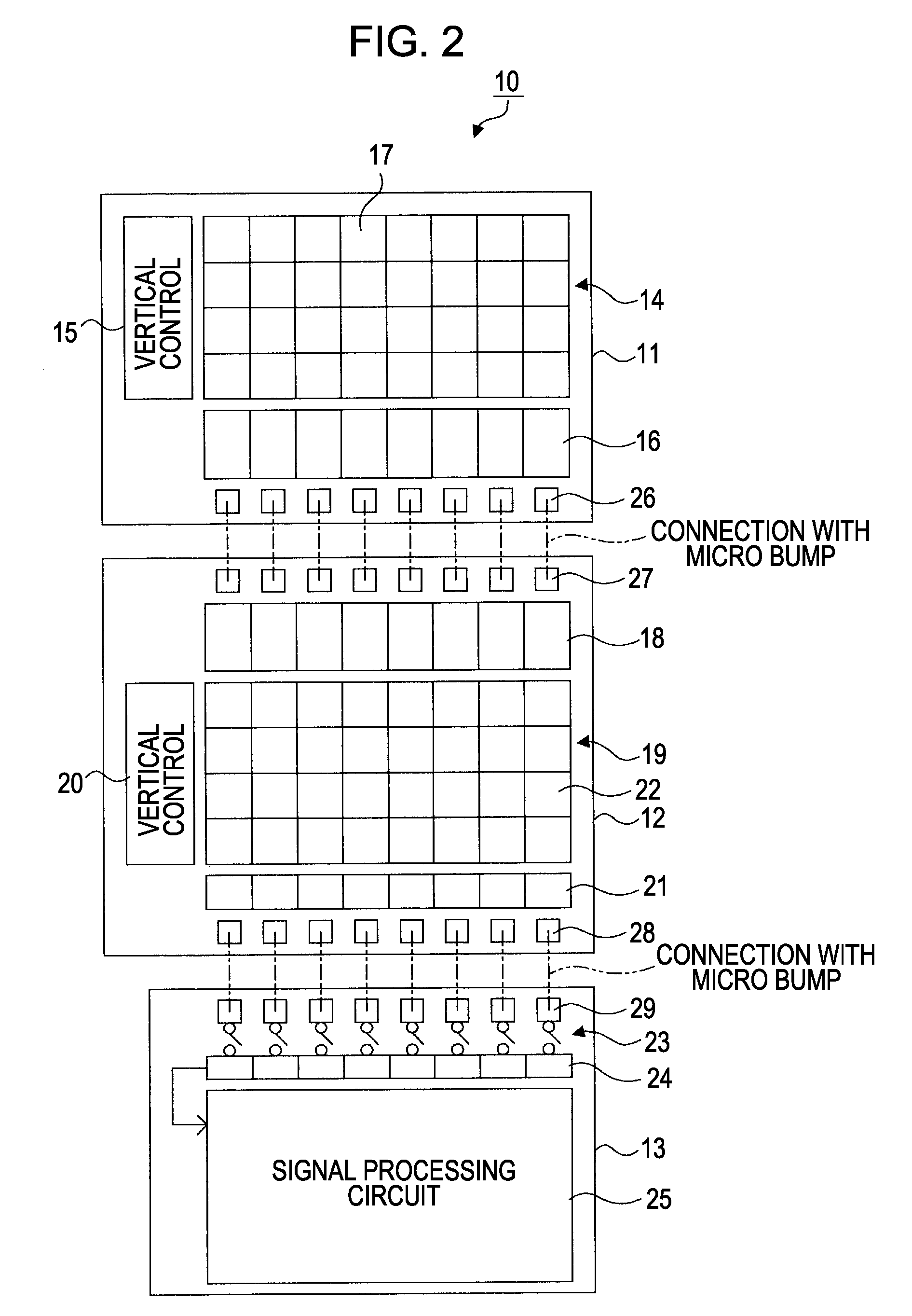
[0026]FIG. 1 is a schematic diagram illustrating an electrical connection state of a solid-state imaging device according to a first embodiment of the present invention. Also, FIG. 2 is a development view illustrating the schematic configuration of the solid-state imaging device according to the first embodiment of the present invention.

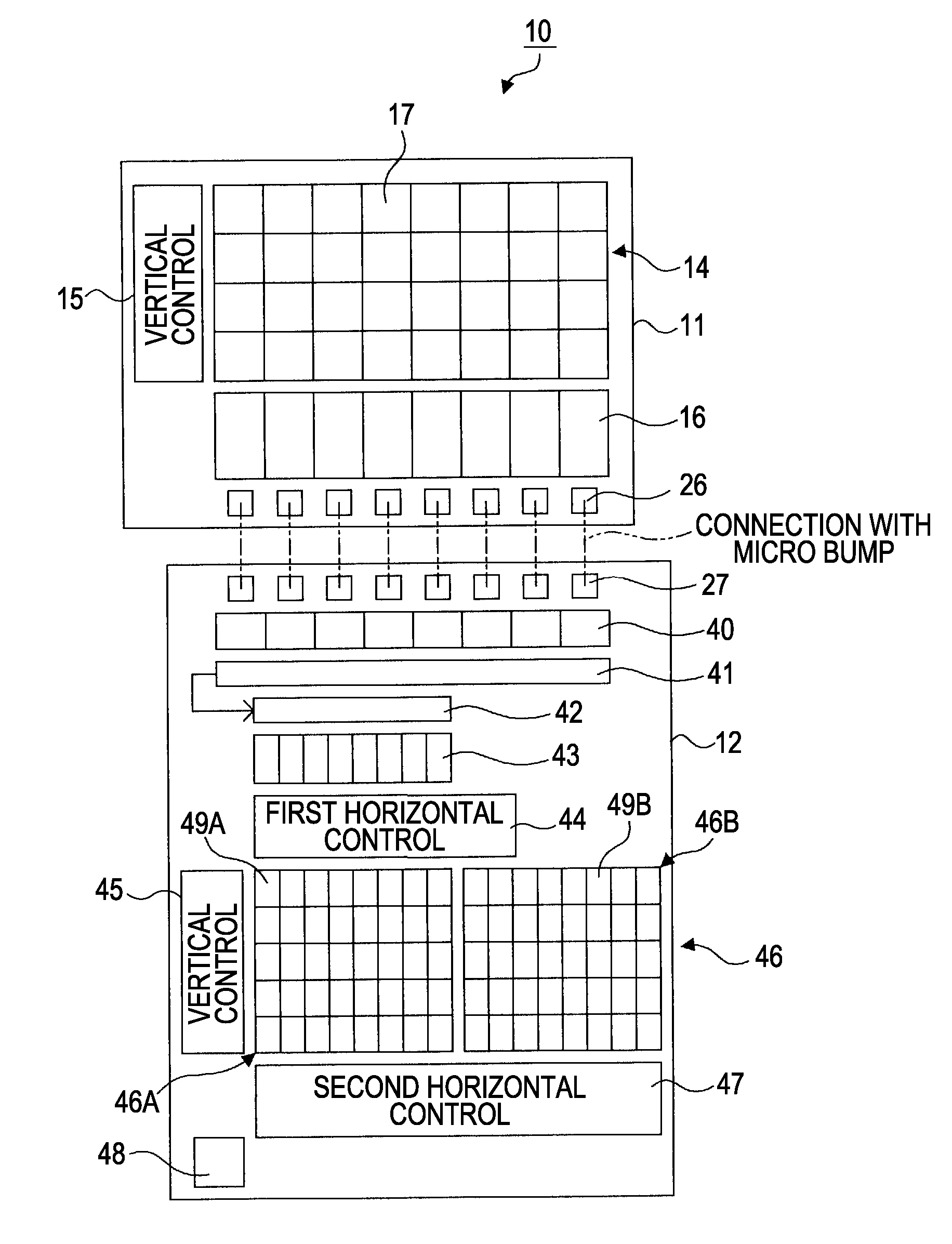
[0027]The solid-state imaging device 10 shown in the figure includes a first semiconductor substrate 11, a second semiconductor substrate 12, and a third semiconductor substrate 13. The first semiconductor substrate 11 is a chip-state substrate (in the following, referred to as a “sensor chip”) on which a CMOS image sensor is mainly mounted. The second semiconductor substrate 12 is a chip-state substrate (in the following, referred to as a “memory chip”) on which a memory circuit is mainly mounted. The third semiconductor substrate 13 is a chip-state substrate (in the following, referred to as a “DSP chip”) on which a DSP circuit is mainly mounted.

[0...

second embodiment

[0048]FIG. 4 is a schematic diagram illustrating an electrical connection state of a solid-state imaging device according to a second embodiment of the present invention. Also, FIG. 5 is a development view illustrating the schematic configuration of the solid-state imaging device according to the second embodiment of the present invention. In this regard, in FIG. 5, the display of the memory chip 12 is omitted. Also, in the second embodiment, the same components as those in the first embodiment are marked with the same reference numerals, and the duplicate description will be omitted.

[0049]In the solid-state imaging device 10, the sensor chip 11 and the DSP chip 13 are connected in parallel (column parallel) by micro bumps for example, for each unit pixel column using one pixel or a plurality of pixels (a few pixels) as one unit. Thus, the pixel signal is transmitted in parallel from the sensor chip 11 to the DSP chip 13. Also, the DSP chip 13 and the memory chip 12 are connected by...

third embodiment

[0057]FIG. 7 is a schematic diagram illustrating an electrical connection state of a solid-state imaging device according to a third embodiment of the present invention. Also, FIG. 8 is a development view illustrating the schematic configuration of the solid-state imaging device according to the third embodiment of the present invention. In this regard, in FIG. 8, the display of the DSP chip 13 is omitted. Also, in the third embodiment, the same components as those in the first embodiment and the second embodiment are marked with the same reference numerals, and the duplicate description will be omitted.

[0058]In the solid-state imaging device 10, the sensor chip 11 and the memory chip 12 are connected in parallel (column parallel) by micro bumps for example, for each unit pixel column using one pixel or a plurality of pixels (a few pixels) as one unit. Thus, the pixel signal is transmitted in parallel from the sensor chip 11 to the memory chip 12. Also, the memory chip 12 and the DS...


PUM


Abstract

A physical-quantity detection device includes at least two semiconductor substrates exchanging a pixel signal read from a pixel-array section including pixels, disposed in a two-dimensional matrix, for converting a physical quantity given from outside into an electrical signal. The two semiconductor substrates have a plurality of terminals connected in parallel and arranged with duplicate pitches with each other in the same direction as a row direction of the pixel-array section, one of the semiconductor substrates transmits the pixel signal to the other of the semiconductor substrates in parallel through the terminals connected in parallel, and the other of the semiconductor substrates scans the transmitted pixel signal to input the signal to a next stage circuit.

Description

CROSS REFERENCES TO RELATED APPLICATIONS[0001]The present invention contains subject matter related to Japanese Patent Application JP 2006-223879 filed in the Japanese Patent Office on Aug. 21, 2006, the entire contents of which are incorporated herein by reference.BACKGROUND OF THE INVENTION[0002]1. Field of the Invention[0003]The present invention relates to a physical-quantity detection device detecting a physical quantity given from outside, a method of driving the physical-quantity detection device, and an imaging apparatus detecting light given from outside as a physical quantity.[0004]2. Description of the Related Art[0005]Camera systems, such as a video camera, an electronic still camera, etc., include a solid-state imaging device including an image sensor having a sensing function for capturing an image, a DSP (digital signal processor) circuit having a signal processing function, a memory circuit having a data-storage function, etc. Also, as shown in FIG. 10, some of the s...

Claims


Application Information

Patent Timeline
IPC IPC(8): H01L27/146G01J1/02H01L25/04H01L25/18H01L27/14H04N5/335
CPCH01L27/14634H01L27/14806H01L2224/73204H01L2224/32225H01L2224/16225H01L2924/00H01L2224/05009H01L2224/0557H01L2224/05568H01L2224/05001H01L2924/00014H04N25/79H01L2224/05599H01L2224/05099
Inventor MABUCHI, KEIJI
Owner SONY CORP
Why Eureka
Try Eureka